Processor Architecture
Modern microprocessors are among the most complex systems ever created by humans.
A single silicon chip, roughly the size of a fingernail, can contain several high-performance processors, large cache memories, and the logic required to interface them to external devices.
The instructions supported by a particular processor and their byte-level encodings are known as its instruction set architecture (ISA).
Different “families” of processors, such as Intel IA32 and x86-64, IBM/Freescale Power, and the ARM processor family, have different ISAs. A program compiled for one type of machine will NOT run on another.
There are many different models of processors within a single family. Each manufacturer produces processors of ever-growing performance and complexity, but the different models remain compatible at the ISA level.
Thus, the ISA provides a conceptual layer of abstraction between compiler writers, who need only know what instructions are permitted and how they are encoded, and processor designers, who must build machines that execute those instructions
In this chapter, we take a brief look at the design of processor hardware. We study the way a hardware system can execute the instructions of a particular ISA.
One important concept is that the actual way a modern processor operates can be quite different from the model of computation implied by the ISA.
- The ISA model would seem to imply sequential instruction execution, where each instruction is fetched and executed to completion before the next one begins.
- By executing different parts of multiple instructions simultaneously, the processor can achieve higher performance than if it executed just one instruction at a time.
- Special mechanisms are used to make sure the processor computes the same results as it would with sequential execution.
- This idea of using clever tricks to improve performance while maintaining the functionality of a simpler and more abstract model is well known in computer science.
There are only fewer than 100 companies worldwide design processor, why should we learn this?
- many design hardware systems that contain processors
- Understanding how the processor works aids in understanding how the overall computer system works.
In this chapter we design a processor to implement a simple ISA call “Y86_64”, which is inspired by x86_64.
The implementation is discribed in HCL(Hardware Control Language), which can be automatically converted into Verilog(Web Aside arch:vlog on page 503) and then produce circuit designs for the microprocessors. We are indeed creating a system that can be realized as hardware.(Although it is no practical value due to its low performance)
We have devised a variety of tools for studying and experimenting with our processor designs
- an assembler for Y86-64
- a simulator for running Y86-64 programs on your machine
- simulators for two sequential and one pipelined processor design.
- The control logic for these designs is described by files in HCL notation.
4.1 The Y86-64 Instruction Set Architecture
Defining an instruction set architecture, such as Y86-64, includes defining the different components of its state, the set of instructions and their encodings, a set of programming conventions, and the handling of exceptional events.
4.1.1 Programmer-Visible State
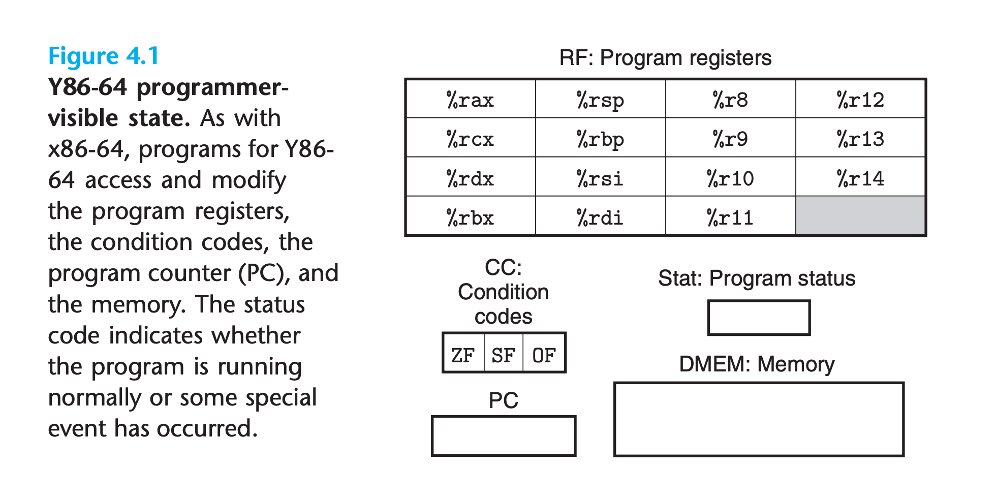
What is programmer visible state
Programmer
Either someone writing programs in assembly code or a compiler generating machine-level code.
Visible state
We do not need to represent and organize this state in exactly the manner implied by the ISA, as long as we can make sure that machine-level programs appear to have access to the programmer-visible state when implementing it.
State
The state for Y86-64 is similar to that for x86-64.
There are 15 program registers, 64 bits
There are three single-bit condition codes,
ZF,SF, andOFThe program counter (PC) holds the address of the instruction currently being executed.
The memory is conceptually a large array of bytes
(Y86-64 programs reference memory locations using virtual addresses, explained in Chatper 9)
a status code
Stat, indicating the overall state of program execution.It will indicate either normal operation or that some sort of exception has occurred, such as when an instruction attempts to read from an invalid memory address
4.1.2 Y86-64 Instructions
The set of Y86-64 instructions is largely a subset of the x86-64 instruction set. It includes only 8-byte integer operations, has fewer addressing modes, and includes a smaller set of operations.
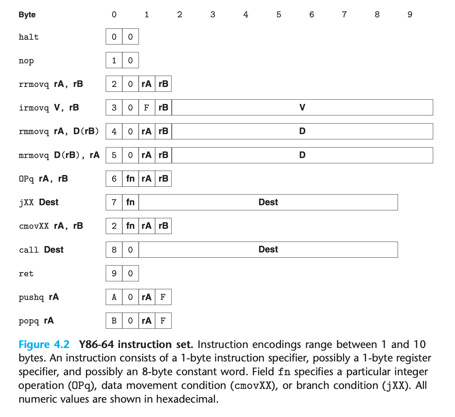
we only use 8-byte data, we can refer to these as “words” without any ambiguity.
assembly-code representation of the instructions on the left and the byte encodings on the right.
We splite
movqinto 4 explicitlyxxmovqinstruction, showing their operands4 integer operation instructions only operate on registers and will set condition codes
7 jump instructions :
jmp, jle, jl, je, jne, jge, jg.6 conditional move instructions :
cmovle, cmovl, cmove, cmovne, cmovge, cmovg, they only work on registerscallandretare same with x86The
haltinstruction stops instruction execution.x86-64 has a comparable instruction, called
hlt, x86-64 application programs are not permitted to use this instruction, since it causes the entire system to suspend operation. For Y86-64, executing the halt instruction causes the processor to stop, with the status code set toHLT.
4.1.3 Instruction Encoding
- Each instruction requires between 1 and 10 bytes, depending on which fields are required
- Every instruction has an initial byte identifying the instruction type.
- This byte is split into two 4-bit parts: the high-order, or code part, and the low-order, or function part.
- code part specify it is in which “instruction class”
- function parts are significant only for the cases where a group of related instructions share a common code.
- Observe that
rrmovqhas the same instruction code as the conditional moves. It can be viewed as an “unconditional move” just as thejmpinstruction is an unconditional jump, both having function code 0.
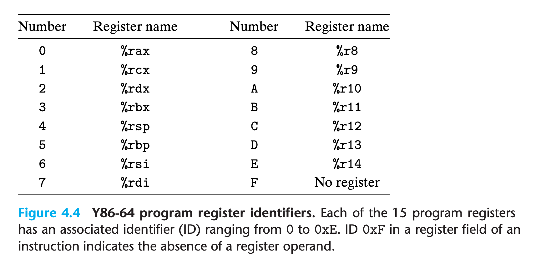
each of the 15 program registers has an associated register identifier (ID) ranging from 0 to 0xE
The numbering of registers in Y86- 64 matches what is used in x86-64. The program registers are stored within the CPU in a register file, a small random access memory where the register IDs serve as addresses.
The optional register specifier can take up one byte, shown in Figure 2
Some instructions require an additional 8-byte constant word
the displacement for
rmmovqandmrmovqaddress specifiersthe destination of branches and calls
(Note that branch and call destinations are given as absolute addresses, rather than using the PC-relative addressing seen in x86-64. Since we are more concerned with simplicity in our presentation, we use absolute addressing. )
As with x86-64, all integers have a little-endian encoding.
(When the instruction is written in disassembled form, these bytes appear in reverse order)
For example, let’s try to encode instruction rmmovq %rsp,0x123456789abcd(%rdx)
rmmovq -> 0x40, first byte%rsp -> 0x4 , %rdx -> 0x2, second byte, register specifier,0x420x123456789abcd, padding to 8 bytes,0x 00 01 23 45 67 89 ab cd, reverse the order to satisfy little endian requirements,0x cd ab 89 67 45 23 01 00- The instruction encode :
0x 40 42 cd ab 89 67 45 23 01 00, note that only integer part need to be little endian !!!
Uniqueness
One important property of any instruction set is that the byte encodings must have a unique interpretation.
An arbitrary sequence of bytes either encodes a unique instruction sequence or is not a legal byte sequence
- This property holds for Y86-64, because every instruction has a unique combination of code and function in its initial byte, and given this byte, we can determine the length and meaning of any additional bytes.
- This property ensures that a processor can execute an objectcode program without any ambiguity about the meaning of the code.
- Even if the code is embedded within other bytes in the program, we can readily determine the instruction sequence as long as we start from the first byte in the sequence.
- On the other hand, if we do not know the starting position of a code sequence, we cannot reliably determine how to split the sequence into individual instructions. This causes problems for disassemblers and other tools that attempt to extract machine-level programs directly from object-code byte sequences.
Practice Problem 4.1
Determine the byte encoding of the Y86-64 instruction sequence that follows. The line
.pos 0x100indicates that the starting address of the object code should be0x100.
2
3
4
5
6
7
irmovq $15,%rbx
rrmovq %rbx,%rcx
loop:
rmmovq %rcx,-3(%rbx)
addq %rbx,%rcx
jmp loop
My solution : :white_check_mark:
1 | 0x100 : 30 f3 0f 00 00 00 00 00 00 00 irmovq $15,%rbx |
Practice Problem 4.2
For each byte sequence listed, determine the Y86-64 instruction sequence it encodes. If there is some invalid byte in the sequence, show the instruction sequence up to that point and indicate where the invalid value occurs. For each sequence, we show the starting address, then a colon, and then the byte sequence.
2
3
4
5
B. 0x200: a06f 800c02000000000000 00 30f30a00000000000000
C. 0x300: 50540700000000000000 10 f0 b01f
D. 0x400: 6113 730004000000000000 00
E. 0x500: 6362 a0 f0
My solution : :white_check_mark:
1 | # A |
4.1.4 Y86-64 Exceptions
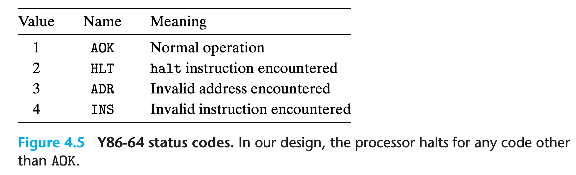
Stat describe the overall state of the executing program
Except AOK, all other codes indicates that some type of exception has occurred.
HLT, indicates that the processor has executed ahaltinstruction.ADR, indicates that the processor attempted to read from or write to an invalid memory address, either while fetching an instruction or while reading or writing data.INS, indicates that an invalid instruction code has been encountered.
For Y86-64, we will simply have the processor stop executing instructions when it encounters any of the exceptions listed. In a more complete design, the processor would typically invoke an exception handler, a procedure designated to handle the specific type of exception encountered.
4.1.5 Y86-64 Programs
1 | long sum(long *start, long count) |
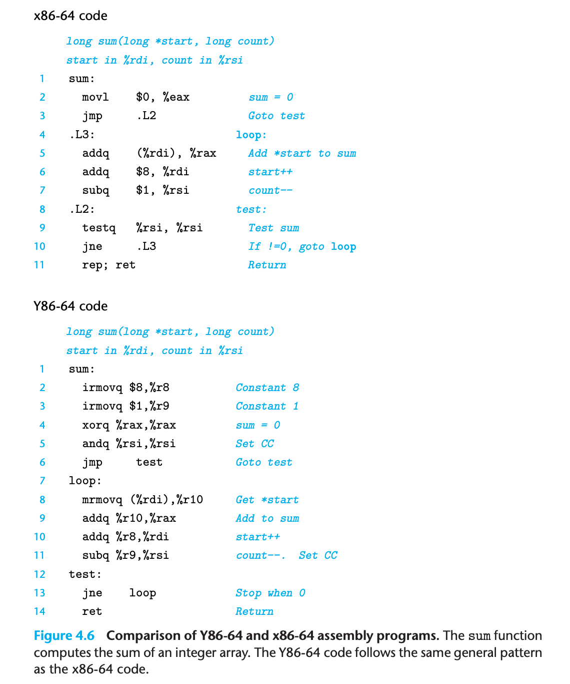
The Y86-64 code loads constants into registers (lines 2–3), since it cannot use immediate data in arithmetic instructions.
So it store the constants into register and then use them as constants
The Y86-64 code requires two instructions (lines 8–9) to read a value from memory and add it to a register, whereas the x86-64 code can do this with a single addq instruction (line 5).
Our hand-coded Y86-64 implementation takes advantage of the property that the subq instruction (line 11) also sets the condition codes, and so the testq instruction of the gcc-generated code (line 9) is not required.
For this to work, though, the Y86-64 code must set the condition codes prior to entering the loop with an andq instruction (line 5).
Sample program
.posis a assembler directive, which tell the assembler to adjust the address at which it is generating code or to insert some words of data.The directive
.pos 0(line 2) indicates that the assembler should begin generating code starting at address 0.The next instruction (line 3) initializes the stack pointer.(defined at line 40, with
.pos 0x200)Lines 8 to 13 of the program declare an array of four words
As this example shows, since our only tool for creating Y86-64 code is an assembler, the programmer must perform tasks we ordinarily delegate to the compiler, linker, and run-time system.
1 | $ ./yas main.ys |
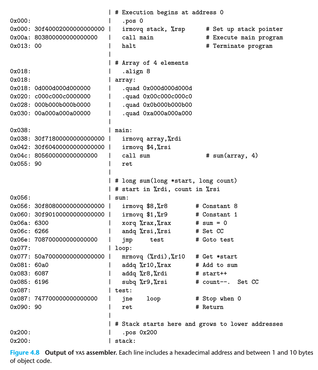
1 | $ ./yis main.yo |
- The first line of the simulation output summarizes the execution and the resulting values of the PC and program status.
- We can see in this output that register
%raxcontains 0xabcdabcdabcdabcd, the sum of the 4-element array passed to proceduresum - In addition, we can see that the stack, which starts at address 0x200 and grows toward lower addresses, has been used, causing changes to words of memory at addresses 0x1f0–0x1f8.
Practice Problem 4.3
One common pattern in machine-level programs is to add a constant value to a register. With the Y86-64 instructions presented thus far, this requires first using an irmovq instruction to set a register to the constant, and then an addq instruction to add this value to the destination register. Suppose we want to add a new instruction iaddq with the following format:
This instruction adds the constant value V to register rB.
Rewrite the Y86-64 sum function of Figure 4.6 to make use of the iaddq instruction. In the original version, we dedicated registers
%r8and%r9to hold constant values. Now, we can avoid using those registers altogether.
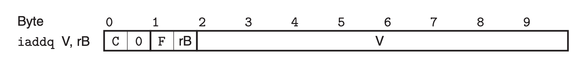
My solution: :white_check_mark:
1 | iaddq $8,%rdi |
Verification:
1 | Stopped in 34 steps at PC = 0x13. Status 'HLT', CC Z=1 S=0 O=0 |
4.1.6 Some Y86-64 Instruction Details
The pushq instruction both decrements the stack pointer by 8 and writes a register value to memory. It is therefore not totally clear what the processor should do when executing the instruction pushq %rsp, since the register being pushed is being changed by the same instruction
We can either push the original value of %rsp or push the decrease value of %rsp
Y86-64 and X86-64 adopt the former one, the original %rsp
Practice Problem 4.7
combine assembly with C in x86
Then you can write code to test the convention used by your machine
1 | .text |
1 | .text |
A similar ambiguity occurs for the instruction popq %rsp. It could either set %rsp to the value read from memory or to the incremented stack pointer.
Y86-64 and X86-64 adopt the former one, the value read from memory
4.2 Logic Design and the Hardware Control Language HCL
Three major components are required to implement a digital system: combinational logic to compute functions on the bits, memory elements to store bits, and clock signals to regulate the updating of the memory elements.
(A complete reference for HCL can be found in Web Aside arch:hcl on page 508.)
4.2.1 Logic Gates
Logic gates are the basic computing elements for digital circuits. They generate an output equal to some Boolean function of the bit values at their inputs.
- Logic gates are always active. If some input to a gate changes, then within some small amount of time, the output will change accordingly.
4.2.2 Combinational Circuits and HCL Boolean Expressions
By assembling a number of logic gates into a network, we can construct computational blocks known as combinational circuits.
Several restrictions are placed on how the networks are constructed:
Every logic gate input must be connected to exactly one of the following:
- one of the system inputs (known as a primary input)(
aandbhere) - the output connection of some memory element
- the output of some logic gate.
- one of the system inputs (known as a primary input)(
The outputs of two or more logic gates cannot be connected together.
Otherwise, the two could try to drive the wire toward different voltages, possibly causing an invalid voltage or a circuit malfunction.
The network must be acyclic.
That is, there cannot be a path through a series of gates that forms a loop in the network. Such loops can cause ambiguity in the function computed by the network.
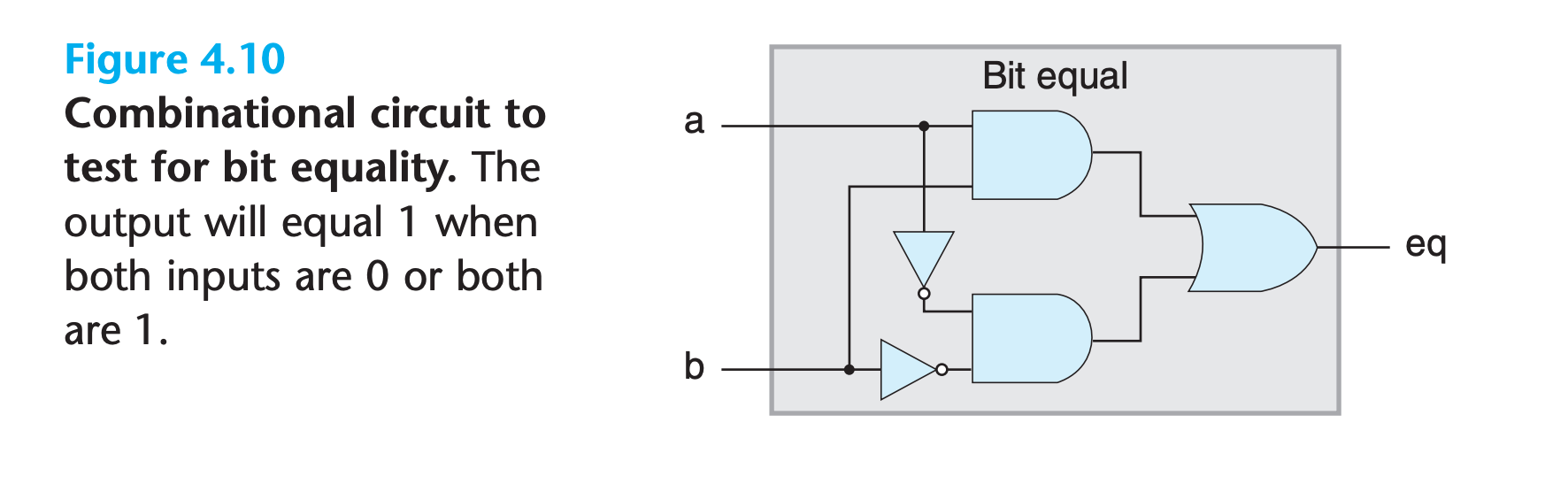
HCL of Figure 4.10
1 | bool eq = (a && b) || (!a && !b); |
- HCL uses C-style syntax, with
=associating a signal name with an expression - Unlike C, however, we do not view this as performing a computation and assigning the result to some memory location. Instead, it is simply a way to give a name to an expression.
Practice Problem 4.9
Write an HCL expression for a signal
xor, equal to the exclusive-or of inputsaandb. What is the relation between the signalsxorandeqdefined above?
My solution : :white_check_mark:
1 | bool xor = (a && !b) || (!a && b); |
1 | xor == !eq |
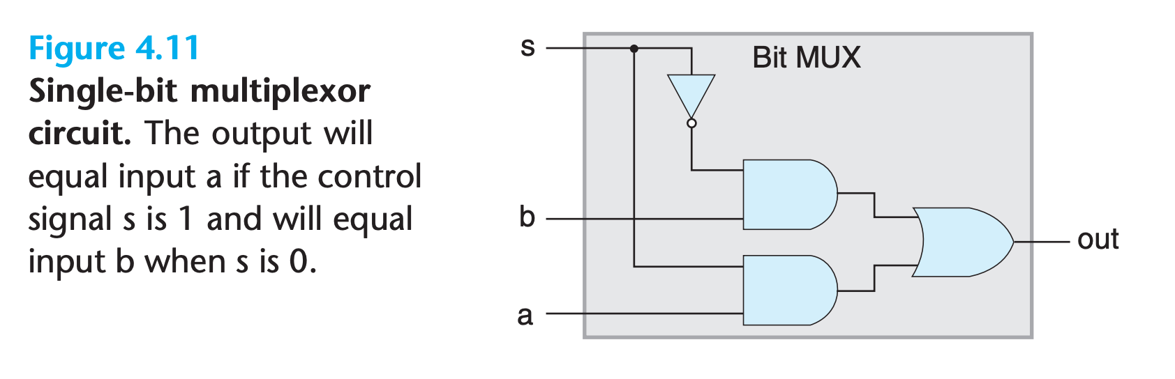
A multiplexor, selects a value from among a set of different data signals, depending on the value of a control input signal.
1 | bool out = (s && a) || (!s && b); |
Difference between HCL and C
- In HCL, if some input to the circuit changes, then after some delay, the outputs will change accordingly. By contrast, a C expression is only evaluated when it is encountered during the execution of a program.
- Logical expressions in C allow arguments to be arbitrary integers, while HCL only allow 0 and 1
- Logical expressions in C have the property that they might only be partially evaluated.(aka short-cut evaluation). HCL doesn’t have this property.
4.2.3 Word-Level Combinational Circuits and HCL Integer Expressions
Combinational circuits that perform word-level computations are constructed using logic gates to compute the individual bits of the output word, based on the individual bits of the input words.
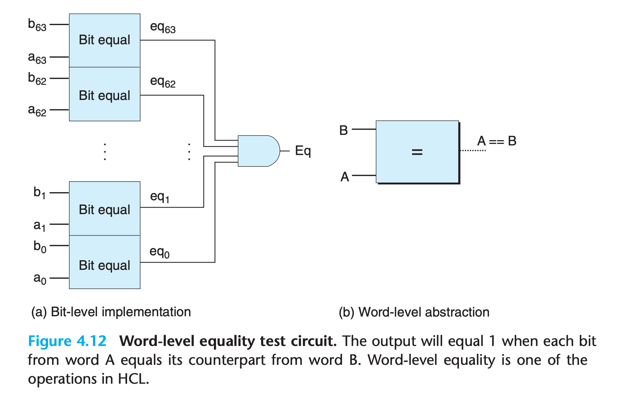
In HCL, we will declare any word-level signal as an
int, without specifying the word size.(This is done for simplicity. In a full-featured hardware description language, every word can be declared to have a specific number of bits)
HCL allows words to be compared for equality
1
bool Eq = (A == B);
Practice Problem 4.10
Suppose you want to implement a word-level equality circuit using the exclusiveor circuits from Problem 4.9 rather than from bit-level equality circuits. Design such a circuit for a 64-bit word consisting of 64 bit-level exclusive-or circuits and two additional logic gates.
My solution : :white_check_mark:
1 | bool Eq = !(xor(a1,b1) || xor(a2,b2) || ... || xor(a64,b64)); |
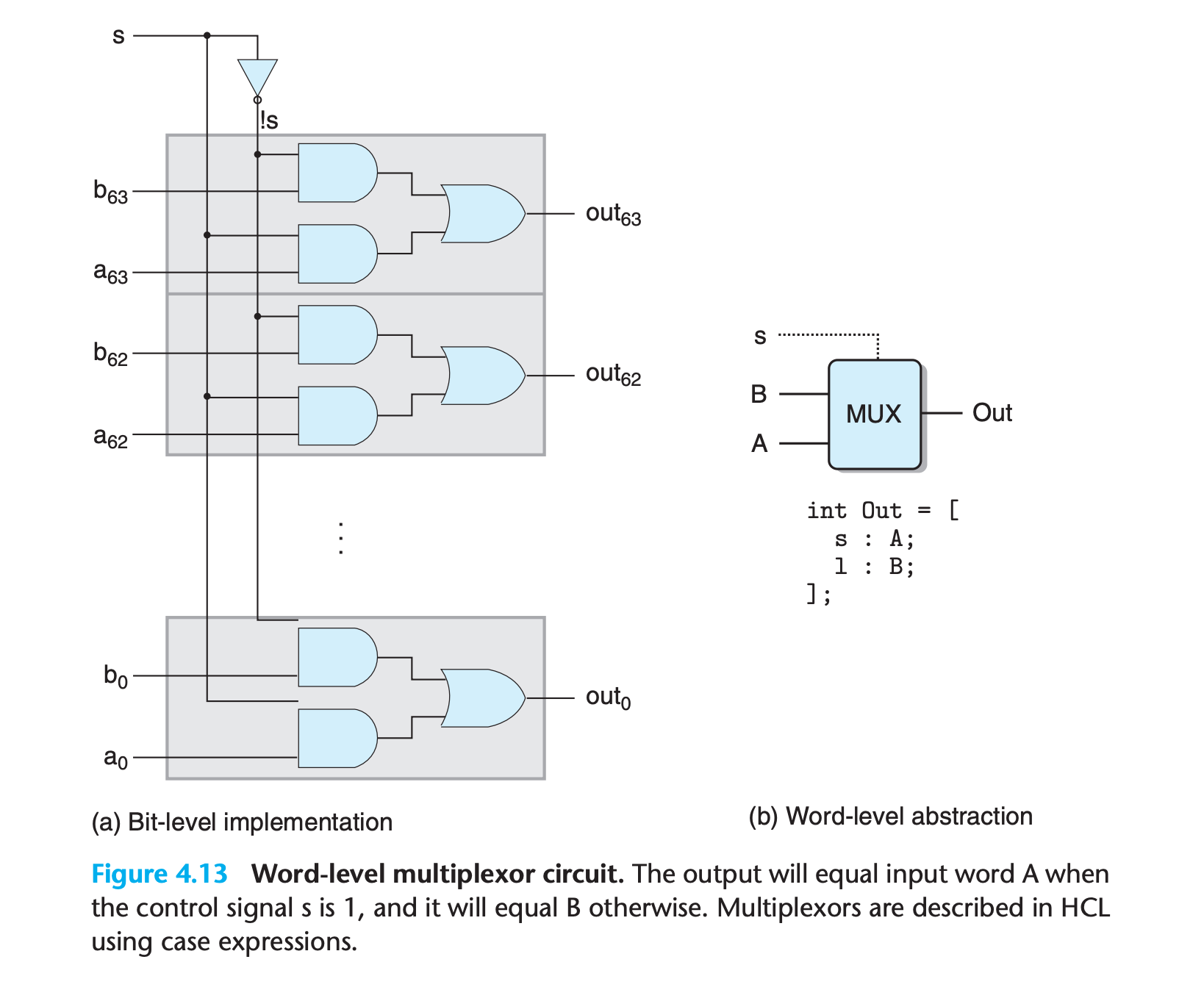
- This circuit generates a 64-bit word Out equal to one of the two input words, A or B, depending on the control input bit s
- Rather than replicating the bit-level multiplexor 64 times, the word-level version reduces the number of inverters by generating
!sonce and reusing it at each bit position.
Multiplexing functions are described in HCL using case expressions. A case expression has the following general form:
1 | [ |
The expression contains a series of cases, where each case i consists of a Boolean expression selecti, indicating when this case should be selected, and an integer expression expri, indicating the resulting value.
Unlike the switch statement of C, we do not require the different selection expressions to be mutually exclusive.
Logically, the selection expressions are evaluated in sequence, and the case for the first one yielding 1 is selected.
So this is the way to specify a default case in HCL
1
2
3
4word Out = [
s : A;
1 : B; // equivalent to default:B
]An actual hardware multiplexor must have mutually exclusive signals controlling which input word should be passed to the output.
(To translate an HCL case expression into hardware, a logic synthesis program would need to analyze the set of selection expressions and resolve any possible conflicts by making sure that only the first matching case would be selected.)
For example
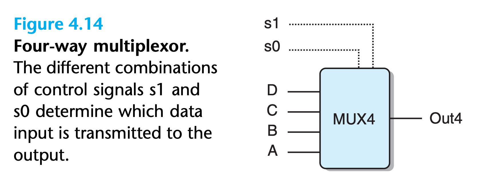
1
2
3
4
5
6word Out4 = [
!s1 && !s0 : A; # 00
!s1 : B; # 01
!s0 : C; # 10
1 : D; # 11
];Observe that the selection expressions can sometimes be simplified, since only the first matching case is selected.
A more complex example
a logic circuit that finds the minimum value among a set of words A, B, and C can be expressed in HCL
1
2
3
4
5word Min3 = [
A <= B && A <= C : A;
B <= A && B <= C : B;
1 : C;
];Practice Problem 4.11
The HCL code given for computing the minimum of three words contains four comparison expressions of the form
X <= Y.Rewrite the code to compute the same result, but using only three comparisons.
My solution: :white_check_mark:
1 | word Min3 = [ |
Practice Problem 4.12
Write HCL code describing a circuit that for word inputs A, B, and C selects the median of the three values. That is, the output equals the word lying between the minimum and maximum of the three inputs
My solution : :x:
Solution on the book:
1 | word Med3 = [ |
Y86 ALU(arithmetic/logical unit)
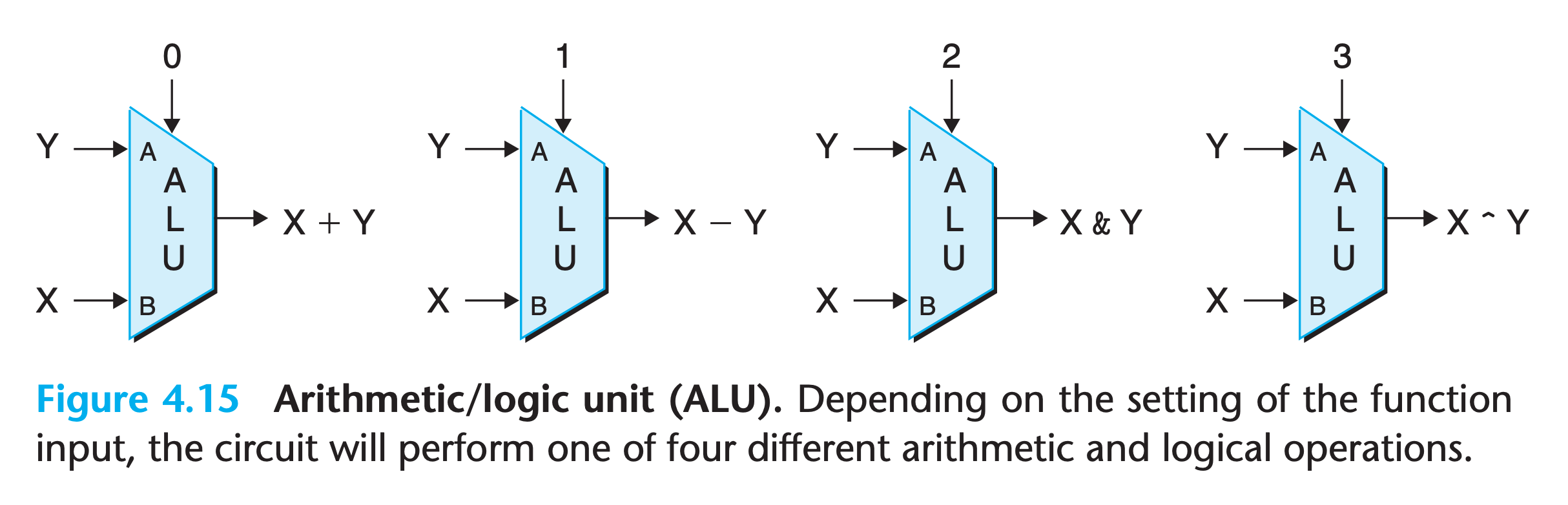
The circuit has three inputs: two data inputs labeled A and B and a control input. Depending on the setting of the control input, the circuit will perform different arithmetic or logical operations on the data inputs.
- Observe that the four operations diagrammed for this ALU correspond to the four different integer operations supported by the Y86-64 instruction set, and the control values match the function codes for these instructions
- Note also the ordering of operands for subtraction, where the A input is subtracted from the B input. This ordering is chosen in anticipation of the ordering of arguments in the
subqinstruction.
4.2.4 Set Membership
Split control signal into bits:
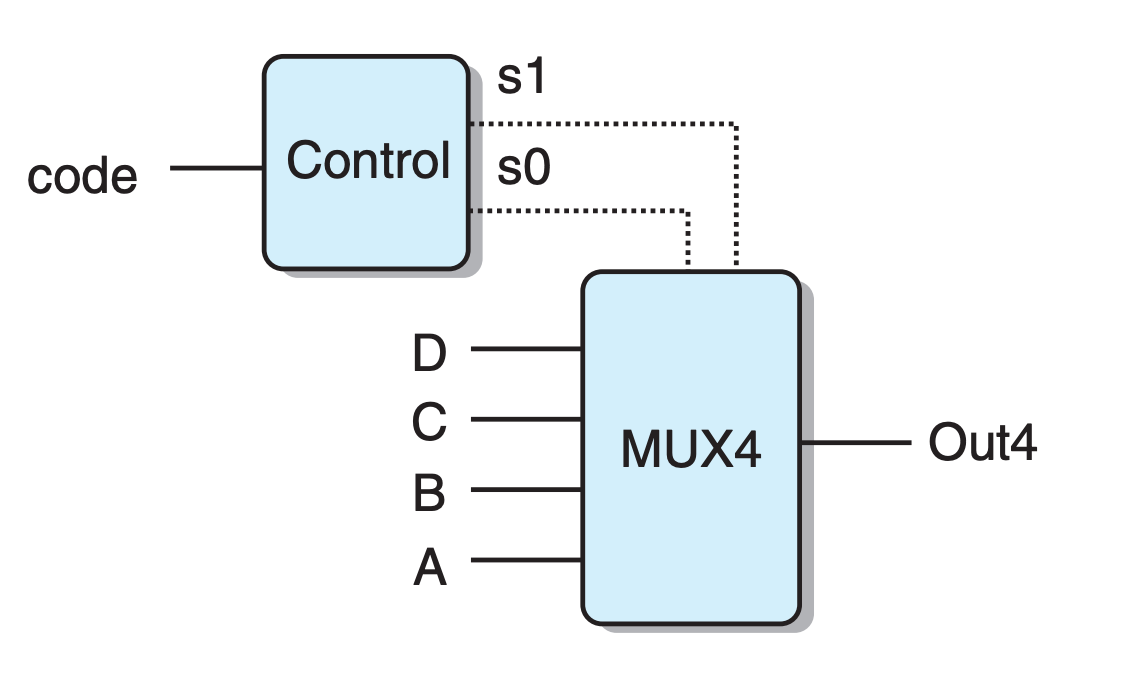
We can express the generation of signals s1 and s0 using equality tests based on the possible values of code:
1 | bool s1 = code == 2 || code == 3; |
A more concise expression can be written that expresses the property that s1 is 1 when code is in the set {2, 3}, and s0 is 1 when code is in the set {1, 3}:
1 | bool s1 = code in { 2, 3 }; |
The general form of a set membership test is
1 | iexpr in {iexpr1, iexpr2, ... , iexprk} |
4.2.5 Memory and Clocking
To create sequential circuits—that is, systems that have state and perform computations on that state—we must introduce devices that store information represented as bits
We consider two classes of memory devices:
Clocked registers (or simply registers) store individual bits or words.
The clock signal controls the loading of the register with the value at its input
Random access memories (or simply memories) store multiple words, using an address to select which word should be read or written.
- Address can be the virtual memory system of a processor
- the register file, where register identifiers serve as the addresses
As we can see, the word “register” means two slightly different things when speaking of hardware versus machine-language programming.When necessary to avoid ambiguity, we will call the two classes of registers “hardware registers” and “program registers,” respectively.
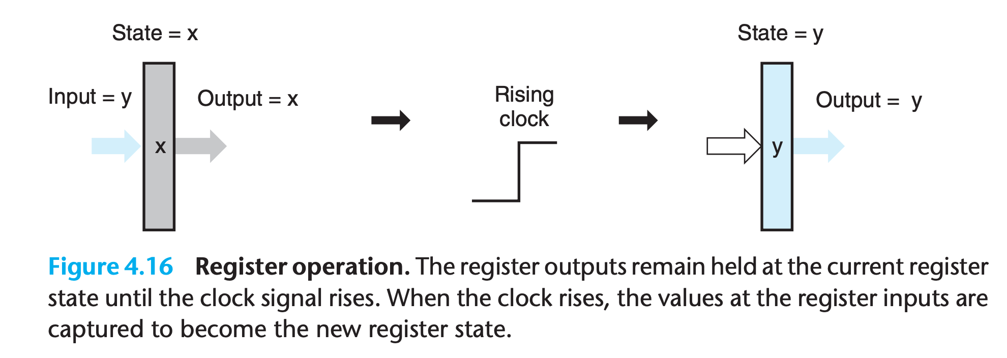
- For most of the time, the register remains in a fixed state (shown as x), generating an output equal to its current state
- Signals propagate through the combinational logic preceding the register, creating a new value for the register input (shown as y), but the register output remains fixed as long as the clock is low.(y is also “latched”)
- As the clock rises, the input signals are loaded into the register as its next state (y), and this becomes the new register output until the next rising clock edge.
- Our Y86-64 processors will use clocked registers to hold the program counter (PC), the condition codes (CC), and the program status (Stat).
Register files
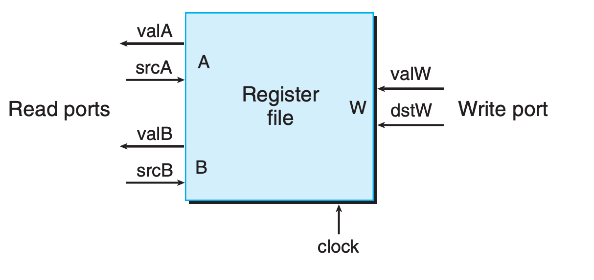
This register file has two read ports, named A and B, and one write port, named W
Such a multiported random access memory allows multiple read and write operations to take place simultaneously
Each port has an address input, indicating which program register should be selected, and a data output or input giving a value for that program register.
Since the register file can be both read and written, a natural question to ask is, “What happens if the circuit attempts to read and write the same register simultaneously?”
The answer is straightforward: if the same register ID is used for both a read port and the write port, then, as the clock rises, there will be a transition on the read port’s data output from the old value to the new
Memory
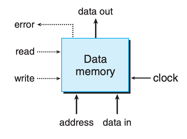
- The error signal will be set to 1 if the address is out of range, and to 0 otherwise
- This signal is generated by combinational logic, since the required bounds checking is purely a function of the address input and does not involve saving any state.
Our processor includes an additional read-only memory for reading instructions. In most actual systems, these memories are merged into a single memory with two ports: one for reading instructions, and the other for reading or writing data.
4.3 Sequential Y86-64 Implementations
As a first step, we describe a processor called SEQ (for “sequential” processor).
- On each clock cycle, SEQ performs all the steps required to process a complete instruction
- This would require a very long cycle time, however, and so the clock rate would be unacceptably low.
4.3.1 Organizing Processing into Stages
In general, processing an instruction involves a number of operations.
We organize them in a particular sequence of stages, attempting to make all instructions follow a uniform sequence, even though the instructions differ greatly in their actions.
The following is an informal description of the stages and the operations performed within them:
- Fetch
The fetch stage reads the bytes of an instruction from memory, using the program counter (PC) as the memory address.
- From the instruction it extracts the two 4-bit portions of the instruction specifier byte, referred to as icode (the instruction code) and ifun (the instruction function)
- Then it can decide the type of the instruction and extract possible required values such as register specifier byte, 8-byte constant word and so on.
- It computes valP to be the address of the instruction following the current one in sequential order. That is, valP equals the value of the PC plus the length of the fetched instruction.
- Decode
The decode stage reads up to two operands from the register file
- Typically, it reads the registers designated by instruction fieldsrA and rB, but for some instructions it reads register %rsp.
- Execute
In the execute stage, the arithmetic/logic unit (ALU) perform one of the following:
- the operation specified by the instruction (according to the value of ifun)
- computes the effective address of a memory reference
- increments or decrements the stack pointer.
The condition codes are possibly set
- For a conditional move instruction, the stage will evaluate the condition codes and move condition (given by ifun) and enable the updating of the destination register only if the condition holds.
- Similarly, for a jump instruction, it determines whether or not the branch should be taken.
- Memory
The memory stage may write data to memory, or it may read data from memory.
- Write back
The write-back stage writes up to two results to the register file
- PC update
The PC is set to the address of the next instruction.
- The processor loops indefinitely, performing these stages
- In our simplified implementation, the processor will stop(
halt) when any exception occurs - Using a very simple and uniform structure is important when designing hardware, since we want to minimize the total amount of hardware (The cost of duplicating blocks of logic in hardware is much higher than the cost of having multiple copies of code in software)
Understand stages via an example
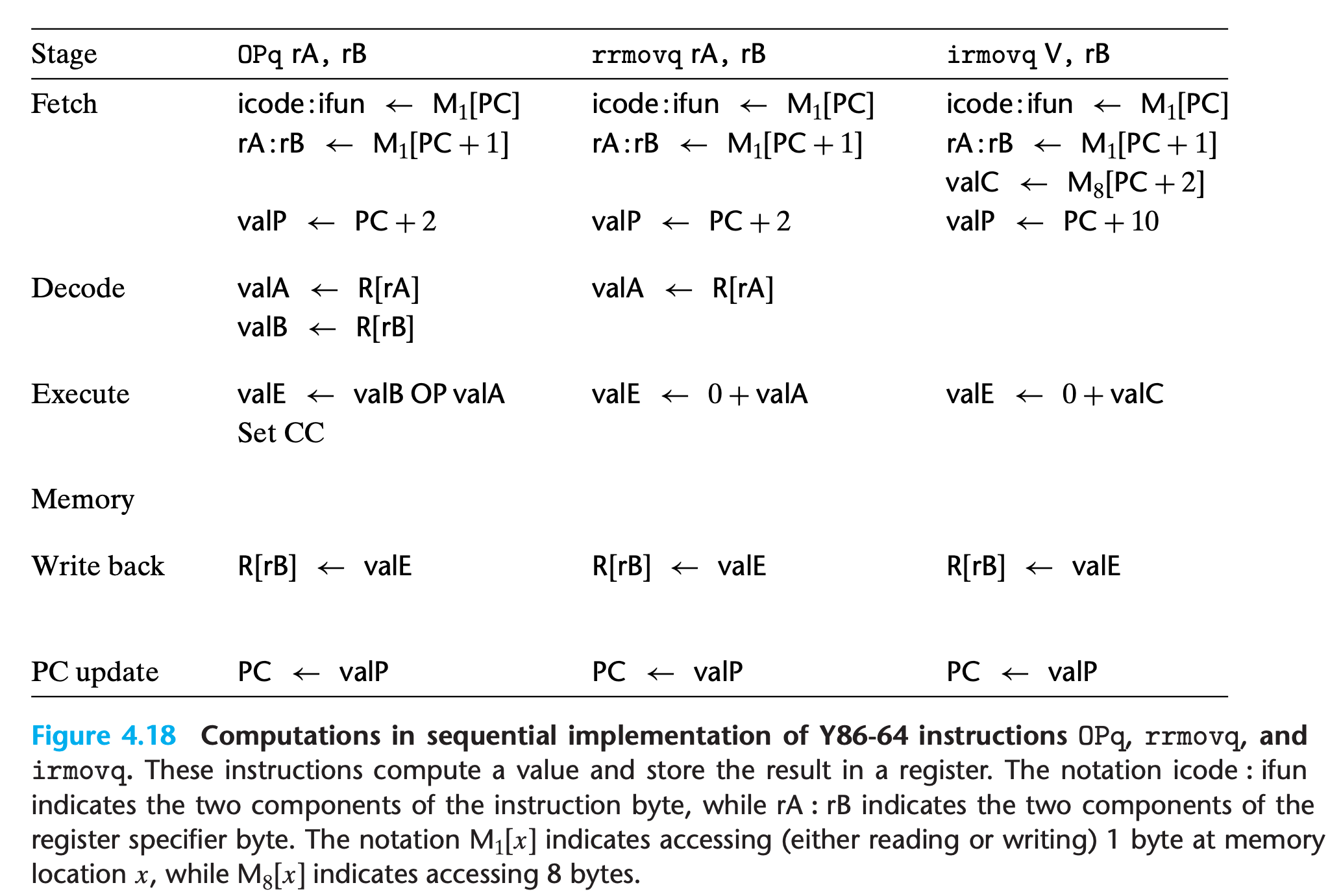
Integer-operation instruction(OPq rA,rB)
- Fetch instruction from memory pointed by
PCand extract register specifier byte - Decode register specifier byte, reading values from registers
- Execute the operation specified by
ifuncpart on retrieved values(set Conditional Code) - Memory stage has nothing to do
- Write back the result of ALU to the destination register
- PC update
Move operation(rrmovq and irmovq)
- Fetch instruction
- Read from register, for
irmovqthere is no register to read from. - Execute an addition of
rAand0orinstant valueand0 - Nothing happens at memory stage
- write back the value to destination register
- PC update
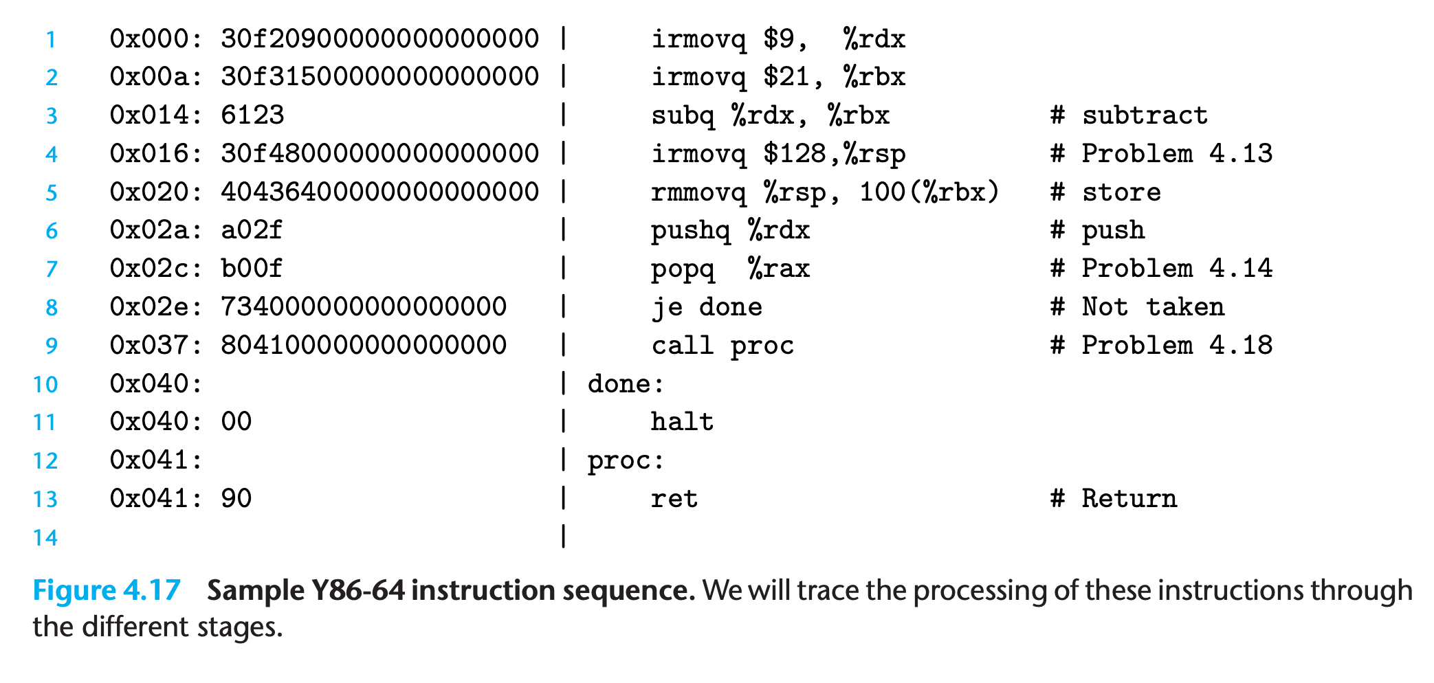
Practice Problem 4.13
Fill in the right-hand column of the following table to describe the processing of the irmovq instruction on line 4 of the object code in Figure 4.17:
2
3
4
5
6
7
8
9
10
11
Stage irmovq V, rB irmovq $128, %rsp
Fetch icode :ifun ← M1[PC]
rA :rB ← M1[PC + 1]
valC ← M8[PC + 2]
valP ← PC + 10
Decode
Execute valE ← 0 + valC
Memory
Write back R[rB] ← valE
PC update PC ← valPHow does this instruction execution modify the registers and the PC?
My solution : :white_check_mark:
1 | Generic Specific |
The instruction set %rsp to 0x80 and update PC to 0x20
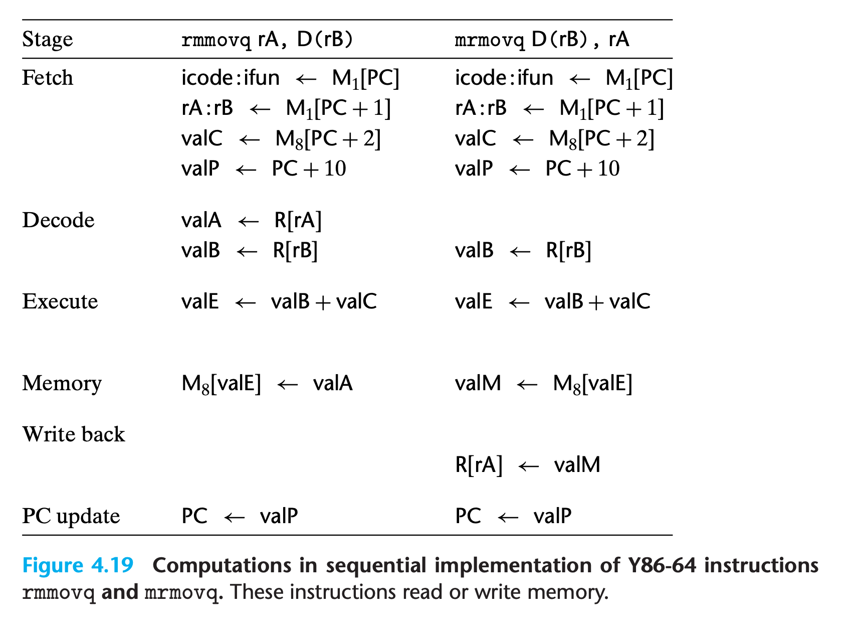
Memory access instructions
- Fetch instruction and extract specifiers
- read values from registers
- use ALU to compute effictive address
- Read from/write to memory
- Write back to register in
mrmovq - update PC
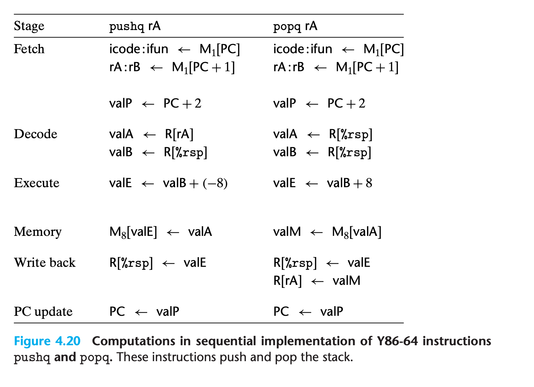
Computation of stack operation(pushq and popq)
- Fetch instruction and extract
rA - read from
R[ra]inpushqand read the value of%rspin both of these two instruction !!! - compute either
%rsp + 8or%rsp - 8 - Read a value from memory (No write back before write back stage!)or write a value from register to memory
- Write new
%rsp(and poped value) back to registers - update PC
The stack pointer %rsp doesn’t update until write back stage
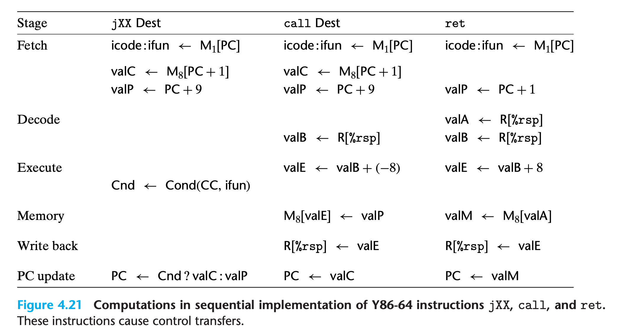
Control transfer instructions (jmp, call and ret)
As with integer operations, we can process all of the jumps in a uniform manner, since they differ only when determining whether or not to take the branch.
- Fetch the instruction, extract the jump target
- No register operation
- test the conditional code and yield a 1-bit
flagvalue, determine jump or not - No memory operation
- No write back
- Set
PC = flag ? target : updatedPC
Practice Problem 4.17
We can see by the instruction encodings (Figures 4.2 and 4.3) that the
rrmovqinstruction is the unconditional version of a more general class of instructions that include the conditional moves. Show how you would modify the steps for therrmovqinstruction below to also handle the six conditional move instructions. You may find it useful to see how the implementation of thejXXinstructions (Figure 4.21) handles conditional behavior.
2
3
4
5
6
7
8
9
10
Fetch icode :ifun ← M1[PC]
rA :rB ← M1[PC + 1]
valP ← PC + 2
Decode valA ← R[rA]
Execute valE ← 0 + valA
Memory
Write back
R[rB] ← valE
PC update PC ← valP
My solution : :white_check_mark:
1 | Stage cmovXX rA, rB |
procedure call and ret
Instructions call and ret bear some similarity to instructions pushq and popq, except that we push and pop program counter values.
- With instruction call, we push valP, the address of the instruction that follows the call instruction. During the PC update stage, we set the PC to valC, the call destination
- With instruction ret, we assign valM, the value popped from the stack, to the PC in the PC update stage.
We have created a uniform framework that handles all of the different types of Y86-64 instructions.
Our task now is to create a hardware design that implements the stages and connects them together.
4.3.2 SEQ Hardware Structure
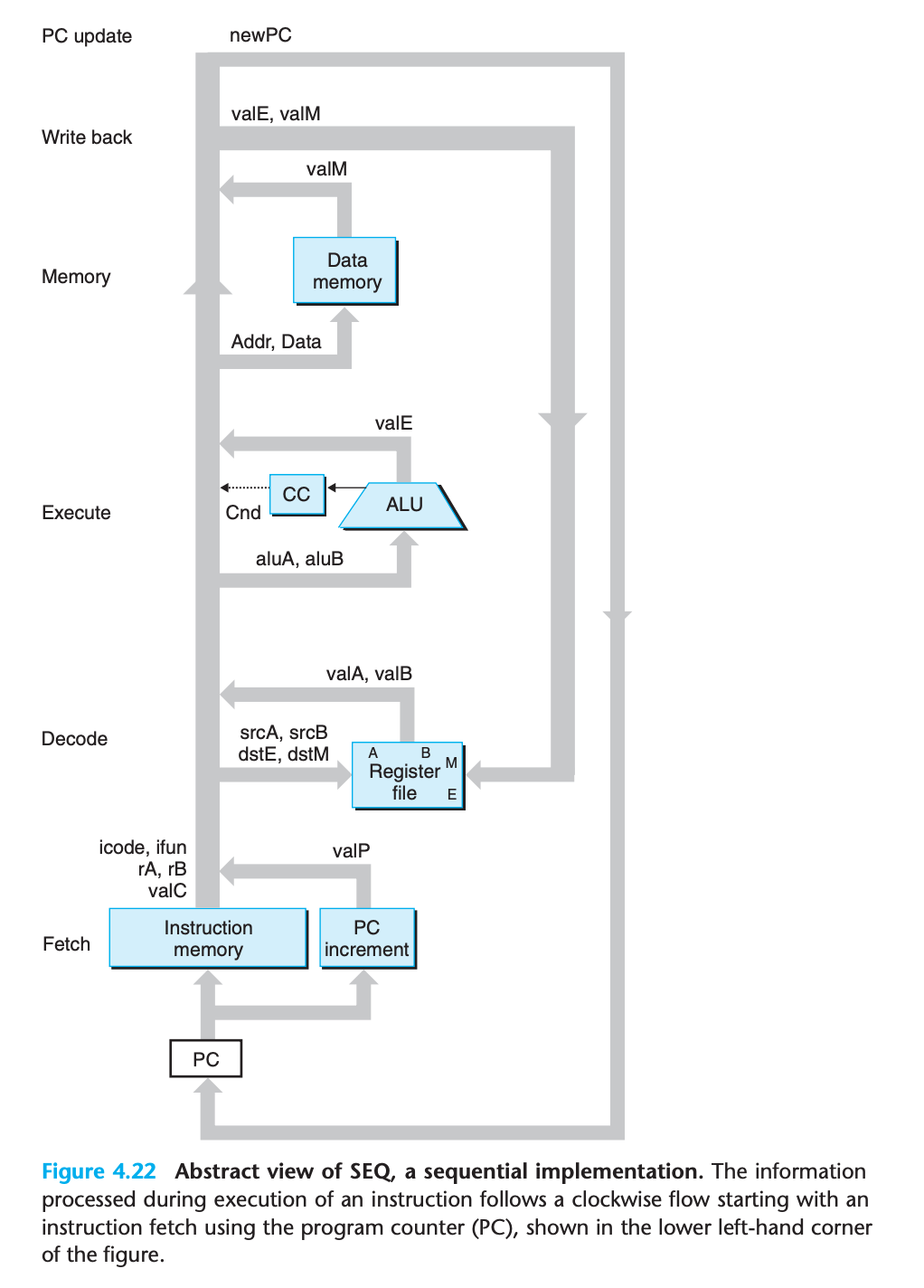
- In SEQ, all of the processing by the hardware units occurs within a single clock cycle
- This diagram omits some small blocks of combinational logic as well as all of the control logic needed to operate the different hardware units and to route the appropriate values to the units. We will add this detail later.
- Our method of drawing processors with the flow going from bottom to top is unconventional. We will explain the reason for this convention when we start designing pipelined processors.
- Fetch
- Using the program counter register as an address, the instruction memory reads the bytes of an instruction.
- The PC incrementer computes valP, the incremented program counter.
- Decode
The register file has two read ports, A and B, via which register values valA and valB are read simultaneously.
- Execute
The execute stage uses the arithmetic/logic (ALU) unit for different purposes according to the instruction type
New values for the condition codes are computed by the ALU
- Memory
The data memory reads or writes a word of memory when executing a memory instruction. The instruction and data memories access the same memory locations, but for different purposes.
- Write back
The register file has two write ports. Port E is used to write values computed by the ALU, while port M is used to write values read from the data memory.
- PC update
The new value of the program counter is selected to be either valP, the address of the next instruction, valC, the destination address specified by a call or jump instruction, or valM, the return address read from memory.
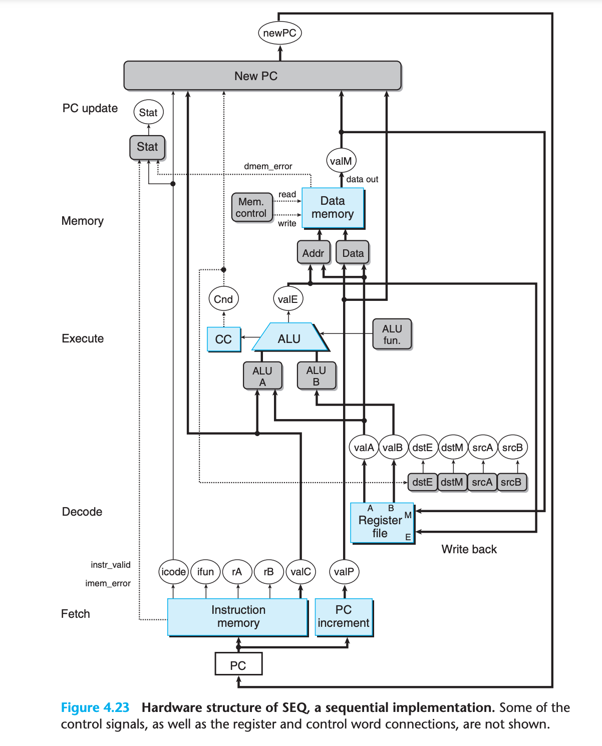
Clocked registers are shown as white rectangles.
The program counter PC is the only clocked register in SEQ.
Hardware units are shown as light blue boxes
We will treat these units as “black boxes” and not go into their detailed designs.
Control logic blocks are drawn as gray rounded rectangles.
These blocks serve to select from among a set of signal sources or to compute some Boolean function. We will examine these blocks in complete detail, including developing HCL descriptions.
Wire names are indicated in white circles.
These are simply labels on the wires, not any kind of hardware element.
Word-wide data connections are shown as medium lines.
Each of these lines actually represents a bundle of 64 wires, connected in parallel, for transferring a word from one part of the hardware to another.
Byte and narrower data connections are shown as thin lines.
Each of these lines actually represents a bundle of four or eight wires, depending on what type of values must be carried on the wires.
Single-bit connections are shown as dotted lines
These represent control values passed between the units and blocks on the chip.
4.3.3 SEQ Timing
the hardware structure of Figure 4.23 operates in a fundamentally different way, with a single clock transition triggering a flow through combinational logic to execute an entire instruction.
Our hardware achieves the same effect as would a sequential execution of the assignments shown in the tables of Figures 4.18 through 4.21, even though all of the state updates actually occur simultaneously and only as the clock rises to start the next cycle.
Because our design follow the principle : No reading back
The processor never needs to read back the state updated by an instruction in order to complete the processing of this instruction.
Execution example
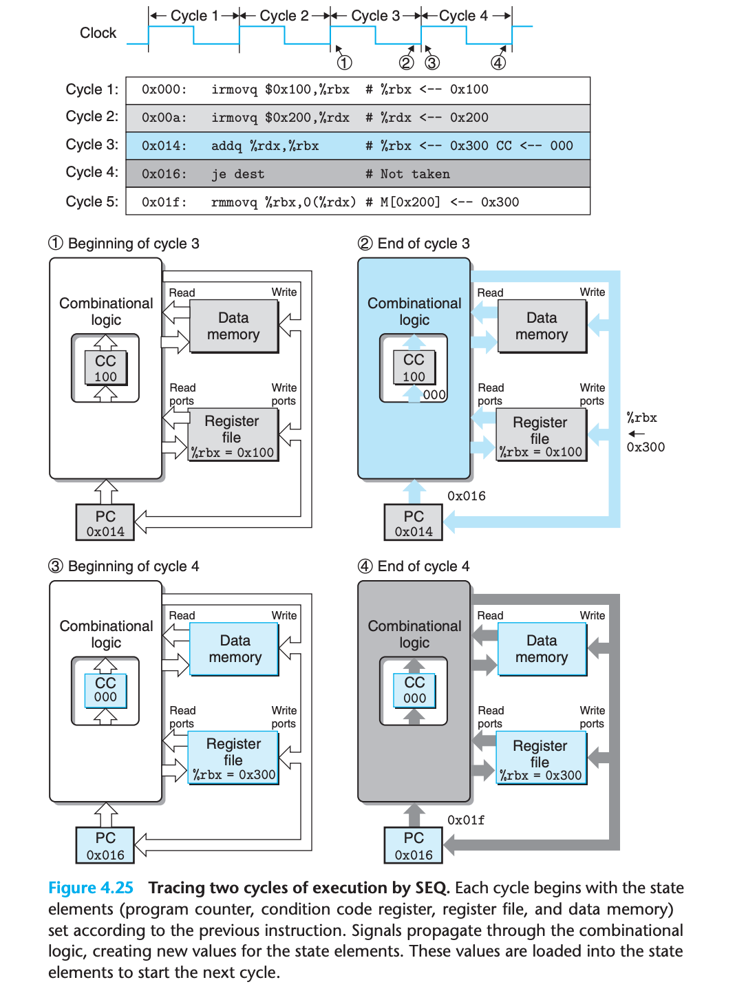
- Read operations propagate through these units as if they were combinational logic, while the write operations are controlled by the clock.
- Every time the clock transitions from low to high, the processor begins executing a new instruction
4.3.4 SEQ Stage Implementations
A complete HCL description for SEQ is given in Web Aside arch:hcl on page 508.
Fetch Stage
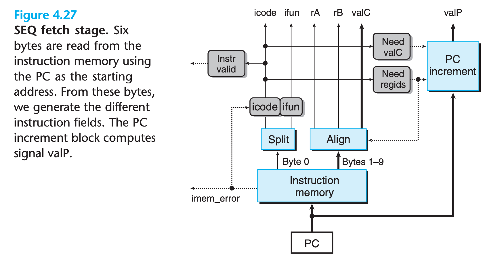
- This unit reads 10 bytes from memory at a time, using the PC as the address of the first byte (byte 0).
- First byte is interpreted as the instruction byte and is split (by the unit labeled “Split”) into two 4-bit quantities
- If the address in PC is invalid, the reading operation will fail(
imem_error) andicodewill be filled with 10, the icode ofnop. - Based on the value of icode, we can compute three 1-bit signals
instr_valid. Does this byte correspond to a legal Y86-64 instruction? This signal is used to detect an illegal instruction.need_regids. Does this instruction include a register specifier byte?need_valC. Does this instruction include a constant word?
As an example, the HCL description for need_regids simply determines whether the value of icode is one of the instructions that has a register specifier byte:
1 | bool need_regids = icode in { IRRMOVQ, IOPQ, IPUSHQ, IPOPQ, |
Practice Problem 4.19
Write HCL code for the signal
need_valCin the SEQ implementation.
My solution : :white_check_mark:
1 | bool need_valC = icode in {IIRMOVQ, IRMMOVQ , IMRMOVQ, IJXX , ICALL}; |
Bytes remaining are processed by the hardware unit labeled “Align” into the register fields and the constant word.
- Byte 1 is split into register specifiers rA and rB when the computed signal need_regids is 1
- If need_regids is 0, both register specifiers are set to 0xF (RNONE), indicating there are no registers specified by this instruction.
The PC incrementer hardware unit generates the signal valP, based on the current value of the PC, and the two signals need_regids and need_valC.
1 | newPC = oldPC + 1 + need_regids + need_valC*8 |
Decode and Write-Back Stages
These two stages are combined because they both access the register file.
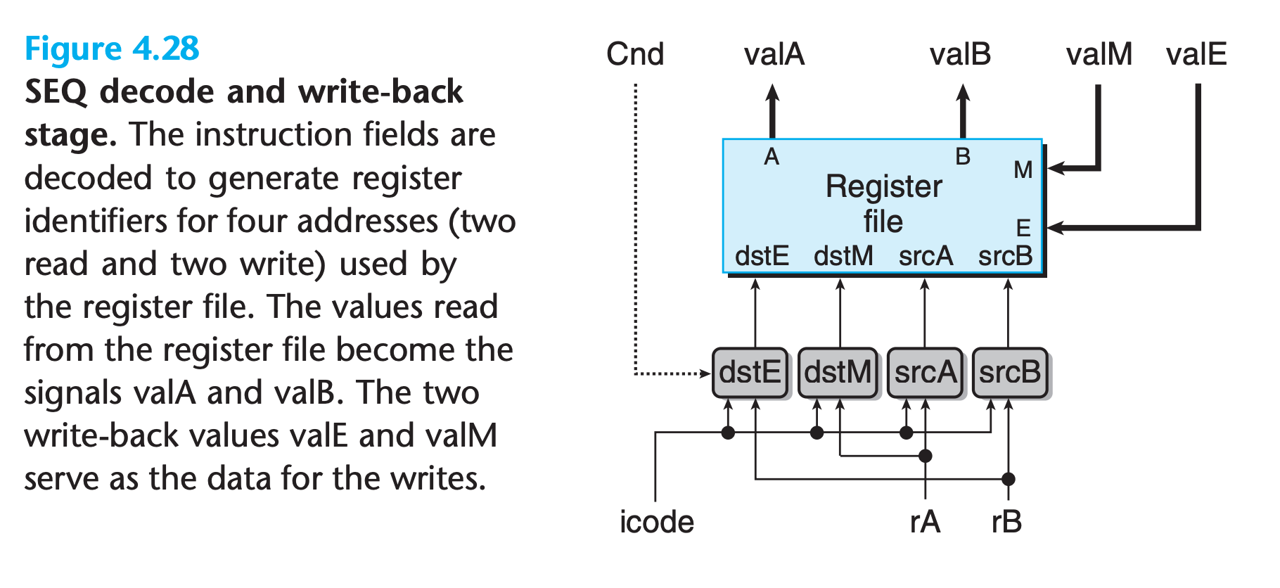
The two read ports have address inputs srcA and srcB, while the two write ports have address inputs dstE and dstM.
The special identifier 0xF (RNONE) on an address port indicates that no register should be accessed.
The address can be computated as follow:
1
2
3
4
5word srcA = [
icode in { IRRMOVQ, IRMMOVQ, IOPQ, IPUSHQ } : rA;
icode in { IPOPQ, IRET } : RRSP;
1 : RNONE; # Don’t need register
];Practice Problem 4.20
The register signal srcB indicates which register should be read to generate the signal valB. The desired value is shown as the second step in the decode stage in Figures 4.18 to 4.21. Write HCL code for srcB.
My solution: :white_check_mark:
1 | word srcA = [ |
Address computation of detE
1 | word dstE = [ |
(We will revisit this signal and how to implement conditional moves when we examine the execute stage)
Execute Stage
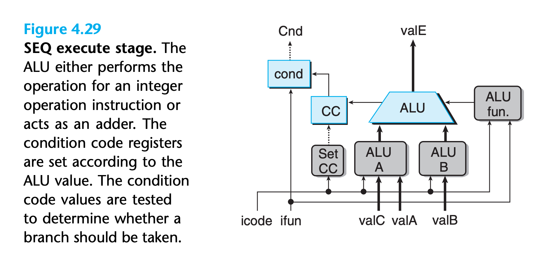
HCL for ALUA
1 | word aluA = [ |
HCL for ALUfun
1 | word alufun = [ |
we only want to set the condition codes when an OPq instruction is executed.We therefore generate a signal set_cc that controls whether or not the condition code register should be updated:
1 | bool set_cc = icode in { IOPQ }; |
The hardware unit labeled “cond” uses a combination of the condition codes and the function code to determine whether a conditional branch or data transfer should take place. We omit the detailed design of this unit.
Memory Stage
The memory stage has the task of either reading or writing program data
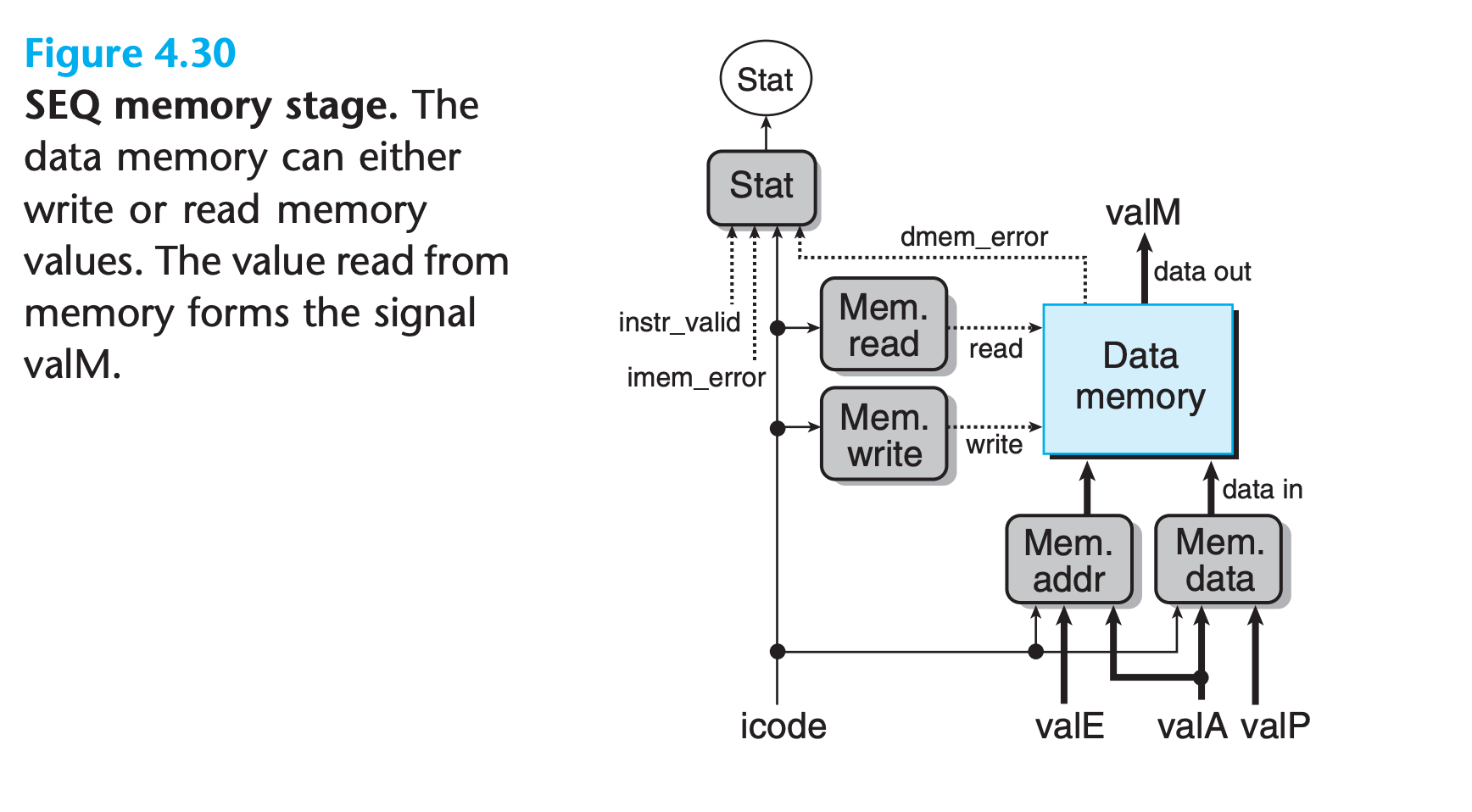
- two control blocks generate the values for the memory address and the memory input data
- Two other blocks generate the control signals indicating whether to perform a read or a write operation.
Observe that the address for memory reads and writes is always valE or valA. We can describe this block in HCL as follows:
1 | word mem_addr = [ |
We want to set the control signal mem_read only for instructions that read data from memory, as expressed by the following HCL code:
1 | bool mem_read = icode in { IMRMOVQ, IPOPQ, IRET }; |
A final function for the memory stage is to compute the status code Stat resulting from the instruction execution according to the values of icode, imem_ error, and instr_valid generated in the fetch stage and the signal dmem_error generated by the data memory
PC Update Stage
The final stage in SEQ generates the new value of the program counter
1 | word new_pc = [ |
Surveying SEQ
- we can implement the entire processor with a small number of different hardware units and with a single clock to control the sequencing of computations.
- The only problem with SEQ is that it is too slow. The clock must run slowly enough so that signals can propagate through all of the stages within a single cycle.
- This style of implementation does not make very good use of our hardware units, since each unit is only active for a fraction of the total clock cycle. We will see that we can achieve much better performance by introducing pipelining.