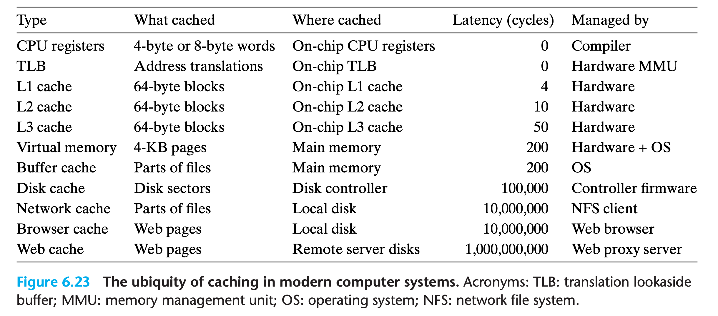
The Memory Hierarchy
In our simple model, the memory system is a linear array of bytes, and the CPU can access each memory location in a constant amount of time.
In practice, a memory system is a hierarchy of storage devices with different capacities, costs, and access times
Memory hierarchies work because well-written programs tend to access the storage at any particular level more frequently than they access the storage at the next lower level.
6.1 Storage Technologies
Much of the success of computer technology stems from the tremendous progress in storage technology.
6.1.1 Random Access Memory(RAM)
Static RAM
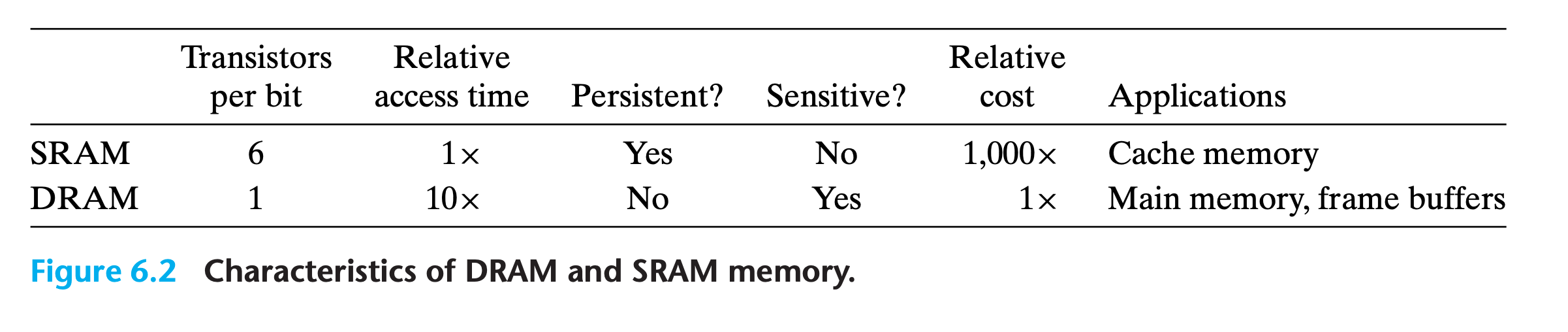
SRAM stores each bit in a bistable memory cell. Each cell is implemented with a six-transistor circuit
- It can stay indefinitely in either of two different voltage configurations, or states
- Any other state will be unstable—starting from there, the circuit will quickly move toward one of the stable states. (Just like an inverted pendulum)
- Due to its bistable nature, an SRAM memory cell will retain its value indefinitely, as long as it is kept powered
- Even when a disturbance, such as electrical noise, perturbs the voltages, the circuit will return to the stable value when the disturbance is removed.
Dynamic RAM
DRAM stores each bit as charge on a capacitor. This capacitor is very small
- Unlike SRAM, however, a DRAM memory cell is very sensitive to any disturbance
- When the capacitor voltage is disturbed, it will never recover.
- Exposure to light rays will cause the capacitor voltages to change.
- Various sources of leakage current cause a DRAM cell to lose its charge within a time period of around 10 to 100 milliseconds
- The memory system must periodically refresh every bit of memory by reading it out and then rewriting it.
Conventional DRAMs
The cells (bits) in a DRAM chip are partitioned into d supercells, each consisting of w DRAM cells
A $d × w$ DRAM stores a total of $dw$ bits of information
The supercells are organized as a rectangular array with r rows and c columns, where $r \times c = d$
Each supercell has an address of the form $(i, j)$, where $i$ denotes the row and $j$ denotes the column
Information flows in and out of the chip via external connectors called pins
(Each pin carries a 1-bit signal.)
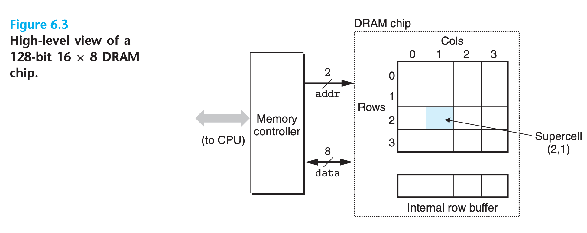
- eight data pins that can transfer 1 byte in or out of the chip, and two addr pins that carry two-bit row and column supercell addresses. Other pins that carry control information are not shown
- Notice that the RAS(Row address Strob) and CAS(Column Address Strob) requests share the same DRAM address pins
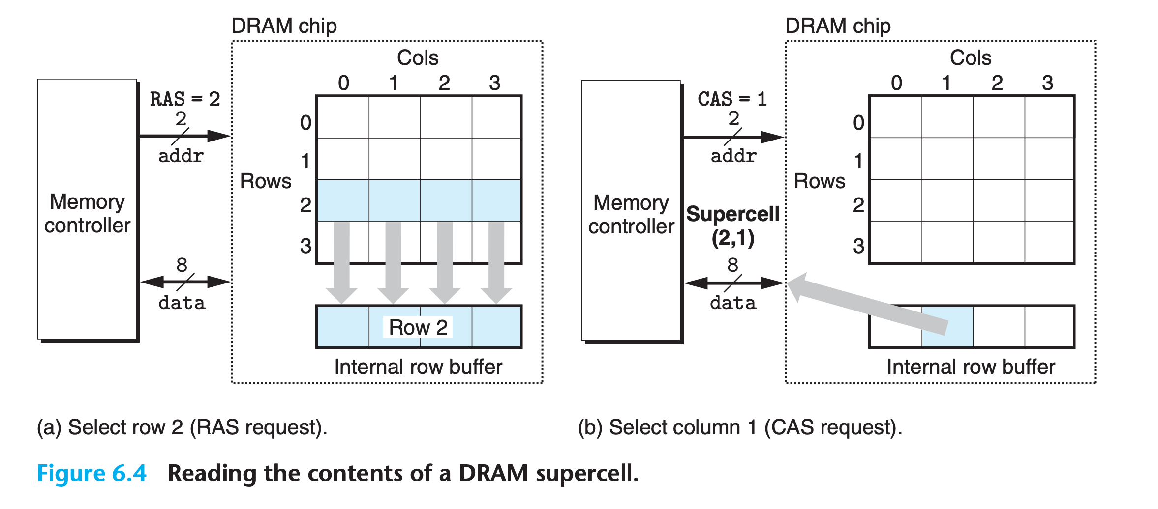
- the memory controller sends row address 2
- The DRAM responds by copying the entire contents of row 2 into an internal row buffer
- the memory controller sends column address 1
- The DRAM responds by copying the 8 bits in supercell (2, 1) from the row buffer and sending them to the memory controller
- One reason circuit designers organize DRAMs as two-dimensional arrays instead of linear arrays is to reduce the number of address pins on the chip
- The disadvantage of the two-dimensional array organization is that addresses must be sent in two distinct steps, which increases the access time.
Memory Modules
DRAM chips are packaged in memory modules that plug into expansion slots on the main system board (motherboard).
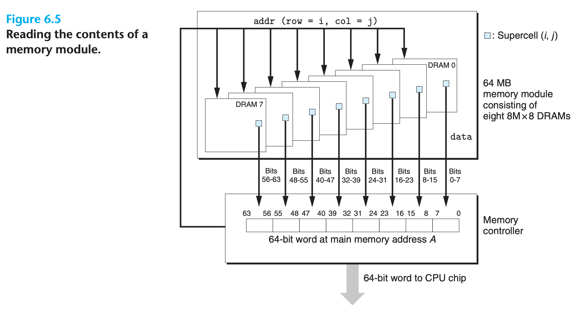
each 64-bit word at byte address A in main memory is represented by the eight supercells whose corresponding supercell address is (i, j)
(One bit in each 2-dimension array)
Main memory can be aggregated by connecting multiple memory modules to the memory controller
- In this case, when the controller receives an address A, the controller selects the module k that contains A, converts A to its (i, j) form, and sends (i, j) to module k.
Practice Problem 6.1
In the following, let $r$ be the number of rows in a DRAM array, $c$ the number of columns, $b_r$ the number of bits needed to address the rows, and $b_c$ the number of bits needed to address the columns. For each of the following DRAMs, determine the power-of-2 array dimensions that minimize $max(b_r, b_c)$, the maximum number of bits needed to address the rows or columns of the array
Organization r c $b_r$ $b_c$ $max(b_r, b_c)$ 16 × 1 16 × 4 128 × 8 512 × 4 1,024 × 4
My solution : :warning:
| Organization | r | c | $b_r$ | $b_c$ | $max(b_r, b_c)$ |
|---|---|---|---|---|---|
| 16 × 1 | 4 | 4 | 2 | 2 | 2 |
| 16 × 4 | 4 | 4 | 2 | 2 | 2 |
| 128 × 8 | 16 | 16 | 4 | 4 | 4 |
| 512 × 4 | 32 | 32 | 5 | 5 | 5 |
| 1,024 × 4 | 32 | 32 | 5 | 5 | 5 |
1 | import math |
We should organize cells as square matrix as possible
Solution on the book :
The idea here is to minimize the number of address bits by minimizing the aspect ratio $max(r, c)/ min(r, c)$. In other words, the squarer the array, the fewer the address bits.
| Organization | r | c | $b_r$ | $b_c$ | $max(b_r, b_c)$ |
|---|---|---|---|---|---|
| 16 × 1 | 4 | 4 | 2 | 2 | 2 |
| 16 × 4 | 4 | 4 | 2 | 2 | 2 |
| 128 × 8 | 16 | 8 | 4 | 3 | 4 |
| 512 × 4 | 32 | 16 | 5 | 4 | 5 |
| 1,024 × 4 | 32 | 32 | 5 | 5 | 5 |
Enhanced DRAMs
There are many kinds of DRAM memories, and new kinds appear on the market with regularity as manufacturers attempt to keep up with rapidly increasing processor speeds.
- Fast page mode DRAM (FPM DRAM)
- Extended data out DRAM (EDO DRAM)
- Synchronous DRAM (SDRAM)
- Double Data-Rate Synchronous DRAM (DDR SDRAM).
- Video RAM (VRAM).
Nonvolatile Memory
DRAMs and SRAMs are volatile in the sense that they lose their information if the supply voltage is turned off. Nonvolatile memories, on the other hand, retain their information even when they are powered off.
For historical reasons, they are referred to collectively as read-only memories (ROMs), even though some types of ROMs can be written to as well as read.
PROM(Programmable ROM)
A PROM can be programmed exactly once. PROMs include a sort of fuse with each memory cell that can be blown once by zapping it with a high current.
EPROM(Erasable PROM)
An EPROM has a transparent quartz window that permits light to reach the storage cells. The EPROM cells are cleared to zeros by shining ultraviolet light through the window
EEPROM(Electronically EPROM)
It does not require a physically separate programming device, and thus can be reprogrammed in-place on printed circuit cards.
Flash memory
Flash memory is a type of nonvolatile memory, based on EEPROMs, that has become an important storage technology.
Programs stored in ROM devices are often referred to as firmware.
Accessing Main Memory
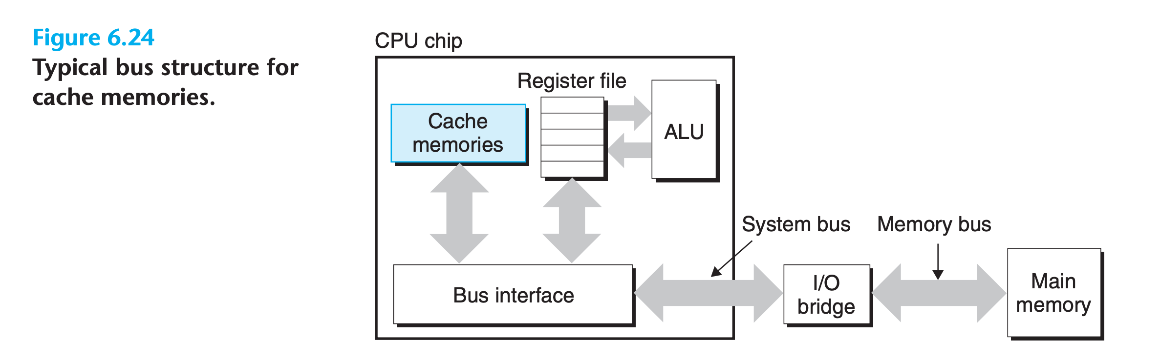
Data flows back and forth between the processor and the DRAM main memory over shared electrical conduits called buses. Each transfer of data between the CPU and memory is accomplished with a series of steps called a bus transaction
- A read transaction transfers data from the main memory to the CPU
- A write transaction transfers data from the CPU to the main memory.
Bus
- A bus is a collection of parallel wires that carry address, data, and control signals
- Depending on the particular bus design, data and address signals can share the same set of wires or can use different sets
- More than two devices can share the same bus.
- The control wires carry signals that synchronize the transaction and identify what kind of transaction is currently being performed
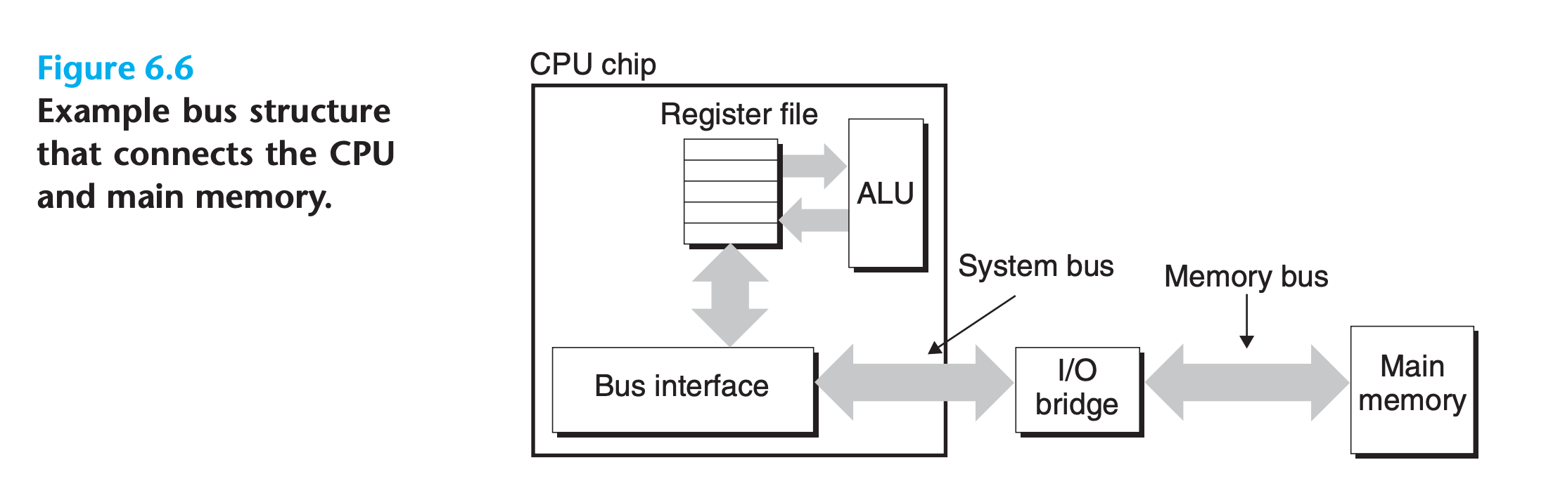
- The I/O bridge translates the electrical signals of the system bus into the electrical signals of the memory bus
- the I/O bridge also connects the system bus and memory bus to an I/O bus that is shared by I/O devices such as disks and graphics cards(Not shown in this graph)
Example of reading and writing main memory
Read
movq A,%rax
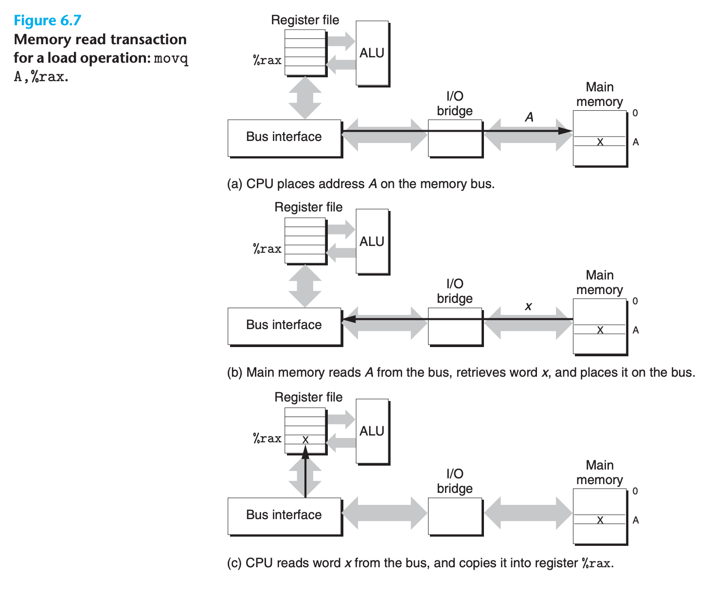
- Circuitry on the CPU chip called the bus interface initiates a read transaction on the bus.
- The CPU places the address A on the system bus. The I/O bridge passes the signal along to the memory bus
- The main memory senses the address signal on the memory bus, reads the address from the memory bus, fetches the data from the DRAM, and writes the data to the memory bus.The I/O bridge translates the memory bus signal into a system bus signal and passes it along to the system bus
- The CPU senses the data on the system bus, reads the data from the bus, and copies the data to register
%rax
Write
movq %rax,A
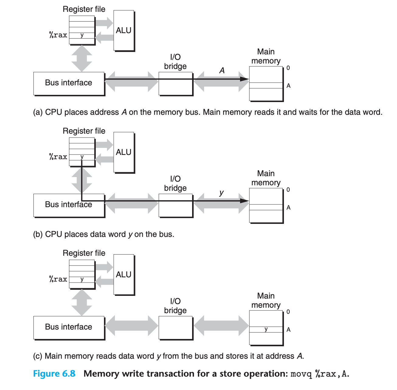
- The CPU initiates a write transaction.
- The CPU places the address on the system bus. The memory reads the address from the memory bus and waits for the data to arrive
- The CPU copies the data in
%raxto the system bus - The main memory reads the data from the memory bus and stores the bits in the DRAM
6.1.2 Disk Storage
Disks are workhorse storage devices that hold enormous amounts of data, on the order of hundreds to thousands of gigabytes. However, it takes on the order of milliseconds to read information from a disk
Disk Geometry
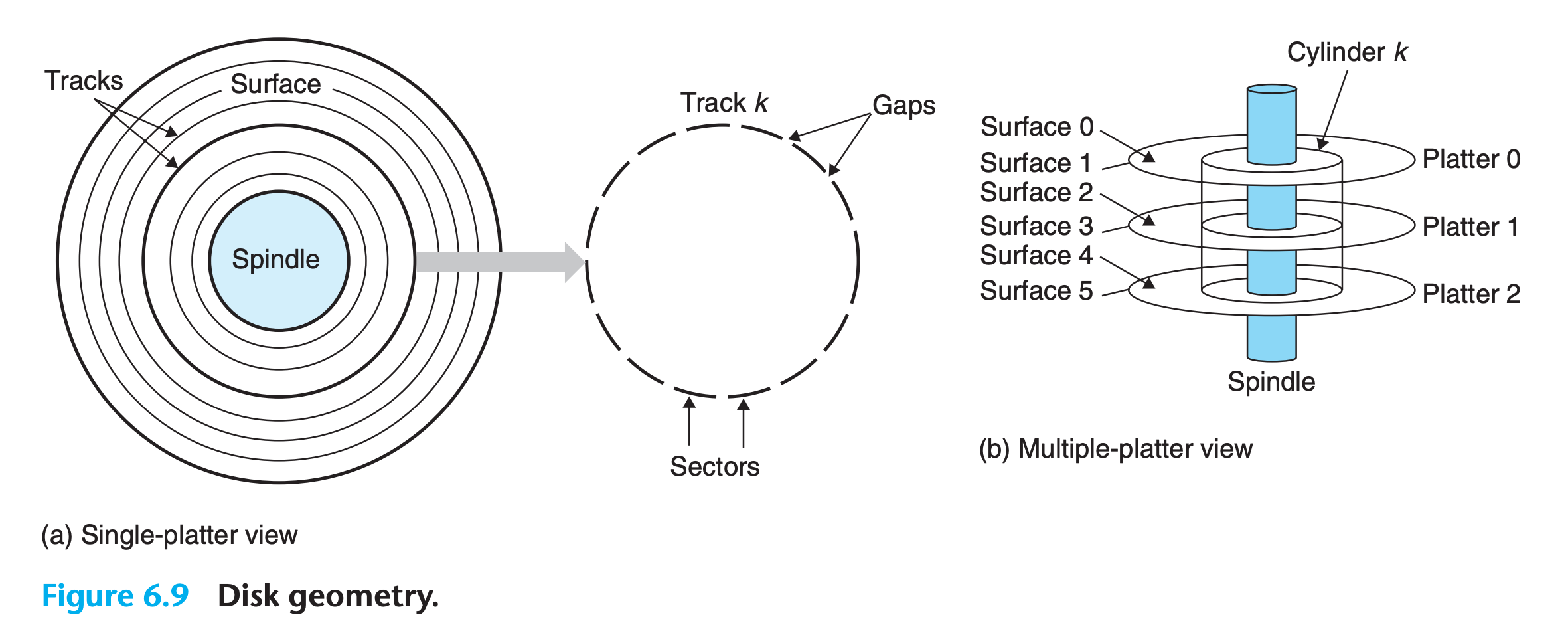
- Disks are constructed from platters
- Each platter consists of two sides, or surfaces, that are coated with magnetic recording material
- A rotating spindle in the center of the platter spins the platter at a fixed rotational rate, typically between 5,400 and 15,000 revolutions per minute (RPM)
- A disk will typically contain one or more of these platters encased in a sealed container
- Each surface consists of a collection of concentric rings called tracks.
- Each track is partitioned into a collection of sectors.
- Each sector contains an equal number of data bits (typically 512 bytes) encoded in the magnetic material on the sector. Sectors are separated by gaps where no data bits are stored. Gaps store formatting bits that identify sectors.
- Disk manufacturers describe the geometry of multiple-platter drives in terms of cylinders, where a cylinder is the collection of tracks on all the surfaces that are equidistant from the center of the spindle
Disk Capacity
The maximum number of bits that can be recorded by a disk is known as its maximum capacity, or simply capacity.
Disk capacity is determined by the following technology factors:
- Recording density (bits/in)
- The number of bits that can be squeezed into a 1- inch segment of a track.
- Track density (tracks/in)
- The number of tracks that can be squeezed into a 1-inch segment of the radius extending from the center of the platter
- Areal density (bits/in2)
- The product of the recording density and the track density.
Old design of disk partitioned every track into the same number of sectors, which was determined by the number of sectors that could be recorded on the innermost track.(without zones)
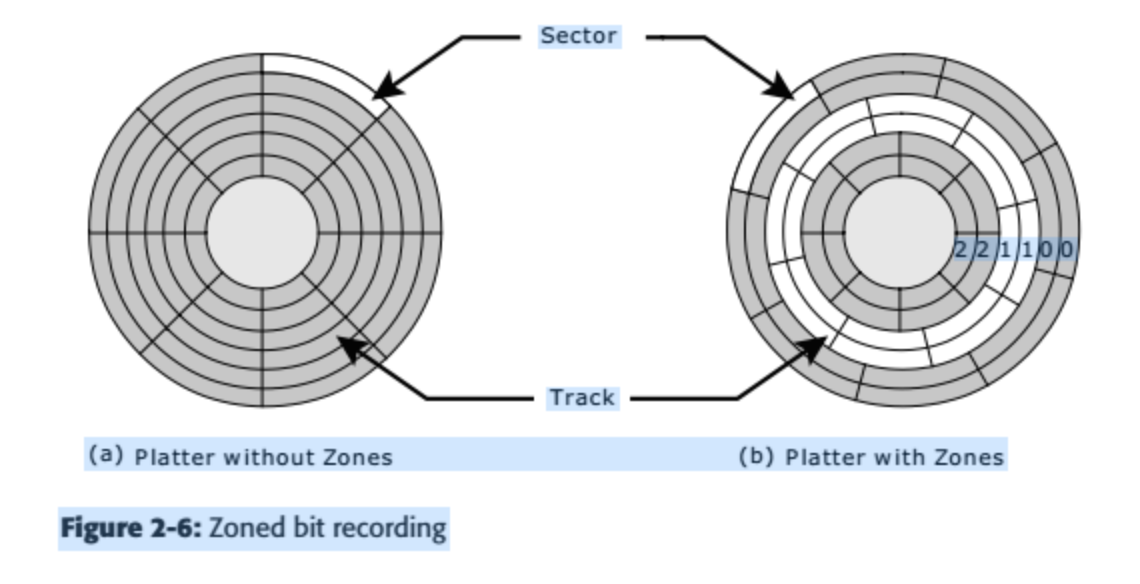
modern high-capacity disks use a technique known as multiple zone recording.Each zone consists of a contiguous collection of cylinders. Each track in each cylinder in a zone has the same number of sectors, which is determined by the number of sectors that can be packed into the innermost track of the zone
The capacity of a disk is given by the following formula:
$$
\text{Capacity} = \frac{bytes}{sector} \times \frac{average \ sectors}{track} \times \frac{tracks}{surface}\times\frac{surfaces}{platter} \times \frac{platters}{disk}
$$
1 | def disk_capacity(bytes_per_sector , average_sectors_per_track , tracks_per_surface , surfaces_per_platter , platters_per_disk): |
Note that manufacturers express disk capacity in units of gigabytes where 1 GB = $10 ^ 9$ bytes rather than $1024^3$
Practice Problem 6.2
What is the capacity of a disk with 3 platters, 15,000 cylinders, an average of 500 sectors per track, and 1,024 bytes per sector?
My solution: :white_check_mark:
1 | platters = 3 |
Disk Operation
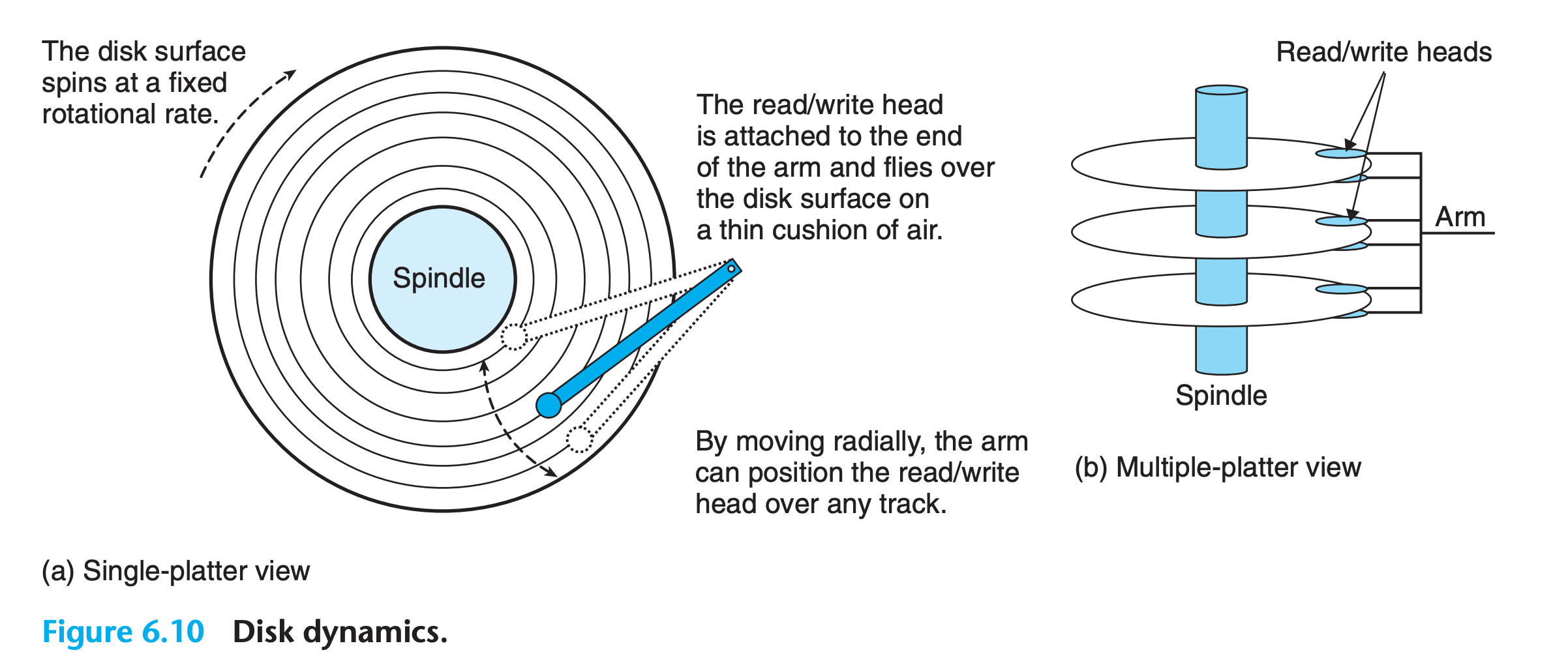
Disks read and write bits stored on the magnetic surface using a read/write head connected to the end of an actuator arm
Once the head is positioned over the desired track, then, as each bit on the track passes underneath, the head can either sense the value of the bit (read the bit) or alter the value of the bit (write the bit).
Disks with multiple platters have a separate read/write head for each surface
The heads are lined up vertically and move in unison. At any point in time, all heads are positioned on the same cylinder.
The read/write head at the end of the arm flies (literally) on a thin cushion of air over the disk surface at a height of about 0.1 microns and a speed of about 80 km/h.
At these tolerances, even a tiny piece of dust on the surface will make the header cease flying and crush into the surface.
For this reason, disks are always sealed in airtight packages.
Disks read and write data in sector-size blocks. The access time for a sector has three main components:
Seek time
- To read the contents of some target sector, the arm first positions the head over the track that contains the target sector.
- The seek time, $T_{seek}$, depends on the previous position of the head and the speed that the arm moves across the surface.
- The average seek time in modern drives, $T_{avg\ seek}$, measured by taking the mean of several thousand seeks to random sectors, is typically on the order of 3 to 9 ms.
Rotational latency
Once the head is in position over the track, the drive waits for the first bit of the target sector to pass under the head
The performance of this step depends on both the position of the surface when the head arrives at the target track and the rotational speed of the disk.
In the worst case, the head just misses the target sector and waits for the disk to make a full rotation
$$
T_{max} = \frac{1}{RPM} \times \frac{60\ secs}{1 \ min}
$$
What is RPM,(the number of turns in one minute)The average rotational latency is simply half of max latency
Transfer time
The transfer time for one sector depends on the rotational speed and the number of sectors per track.
the average transfer time for one sector in seconds
$$
T_{avg\ trans} = \frac{1}{RPM} \times \frac{1}{avg\ sectors} \times \frac{60 \sec}{\min}
$$
We can estimate the average time to access the contents of a disk sector as the sum of the average seek time, the average rotational latency, and the average transfer time.
Practice Problem 6.3
Estimate the average time (in ms) to access a sector on the following disk:
Parameters Values Rotational Rate 12000 RPM T avg seek 5 ms Average number of sectors per track 300
My solution : :white_check_mark:
$$
T_{avg \ seek } = 5 ms
$$
$$
T_{rotational\ latency} = \frac{1}{2} \times\frac{1}{12000} \times \frac{60\ secs}{1 \ min} = 0.0025 \sec = 2.5 ms
$$
$$
T_{trans} = \frac{1}{300} \times \frac{60}{12000}= 0.0167 ms
$$
$$
T = 0.0167 + 5 + 2.5 = 7.516 ms
$$
Logical Disk Blocks
To hide the complex structure from the operating system, modern disks present a simpler view of their geometry as a sequence of B sector-size logical blocks, numbered 0, 1,…,B−1.
A small hardware/firmware device in the disk package, called the disk controller, maintains the mapping between logical block numbers and actual (physical) disk sectors.
- When the operating system wants to perform an I/O operation such as reading a disk sector into main memory, it sends a command to the disk controller asking it to read a particular logical block number
- Firmware on the controller performs a fast table lookup that translates the logical block number into a (surface, track, sector)triple that uniquely identifies the corresponding physical sector
- Hardware on the controller interprets this triple to move the heads to the appropriate cylinder, waits for the sector to pass under the head, gathers up the bits sensed by the head into a small memory buffer on the controller, and copies them into main memory.
Practice Problem 6.4
Suppose that a 1 MB file consisting of 512-byte logical blocks is stored on a disk drive with the following characteristics:
Parameters Values Rotational Rate 13000 RPM T avg seek 6 ms Average number of sectors per track 5000 Surface 4 Secotor Size 512 bytes For each case below, suppose that a program reads the logical blocks of the file sequentially, one after the other, and that the time to position the head over the first block is T avg seek + T avg rotation.
A. Best case: Estimate the optimal time (in ms) required to read the file given the best possible mapping of logical blocks to disk sectors (i.e., sequential).
B. Random case: Estimate the time (in ms) required to read the file if blocks are mapped randomly to disk sectors.
My solution : :white_check_mark:
$$
T_{avg \ rotation} = \frac{1}{2} \times \frac{60}{13000}= \frac{3}{1300} \sec = 2.3 ms
$$
$$
sectors(blocks) = \frac{1 \ MB}{512 \ bytes} = 2048
$$
A:
$$
T_{first\ block} = 6 ms + \frac{30}{13} ms = 8.307 ms
$$
$$
T_{trans\ one \ sector} = \frac{1}{5000} \times \frac{60}{13000} = 9.23\times 10^{-4} \sec
$$
$$
T = T_{first\ block} + 2048 \times T_{trans\ one \ sector} = 1.89 ms
$$
B:
$$
T = (T_{first\ block} + T_{trans\ one\ sector}) \times 2048 = 17014.626304ms\= 17.014 \sec
$$
You can see now why it’s often a good idea to defragment your disk drive!
Connecting I/O Devices
Unlike the system bus and memory buses, which are CPU-specific, I/O buses are designed to be independent of the underlying CPU.
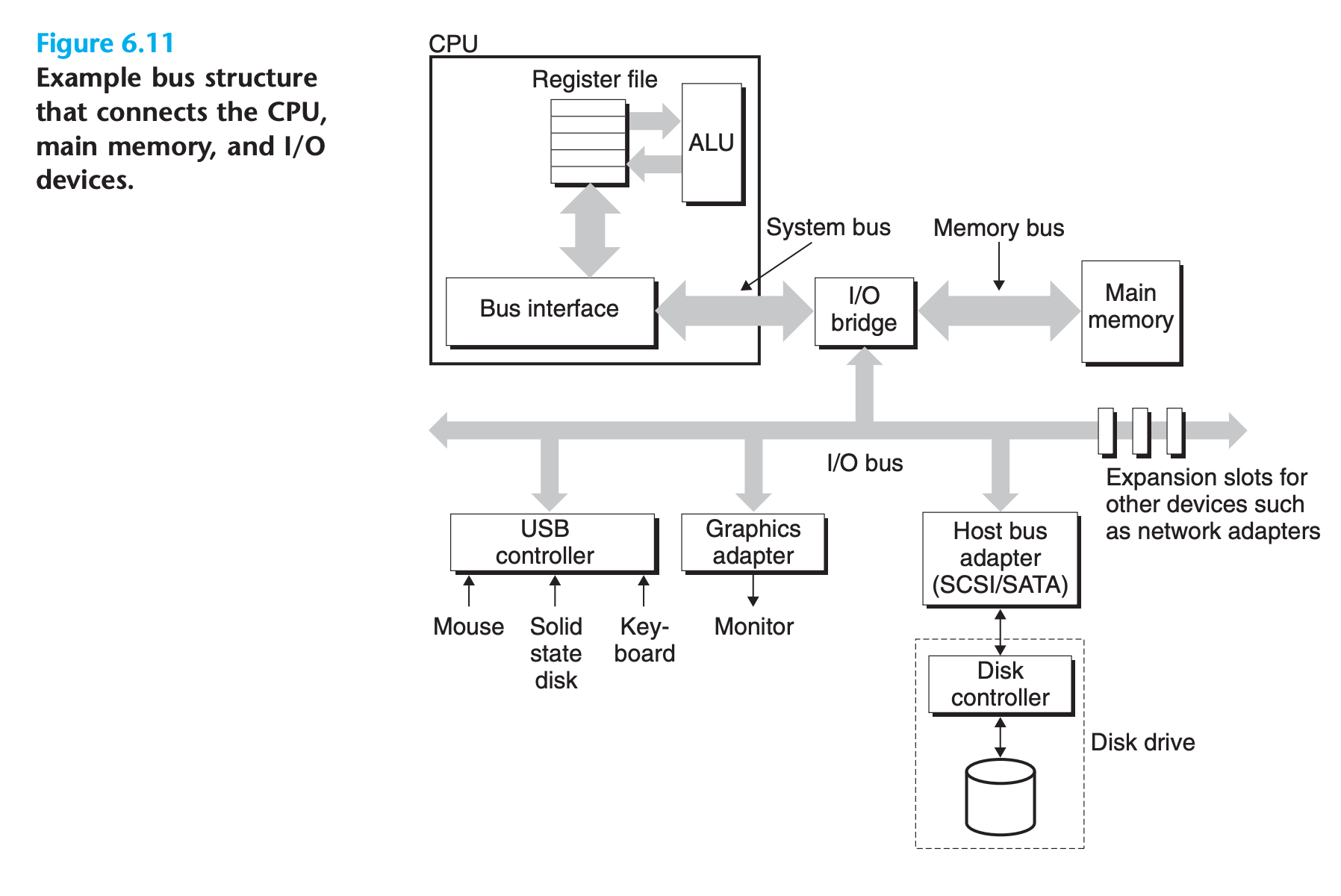
- Although the I/O bus is slower than the system and memory buses, it can accommodate a wide variety of third-party I/O devices
- Additional devices such as network adapters can be attached to the I/O bus by plugging the adapter into empty expansion slots on the motherboard that provide a direct electrical connection to the bus.
Accessing Disks
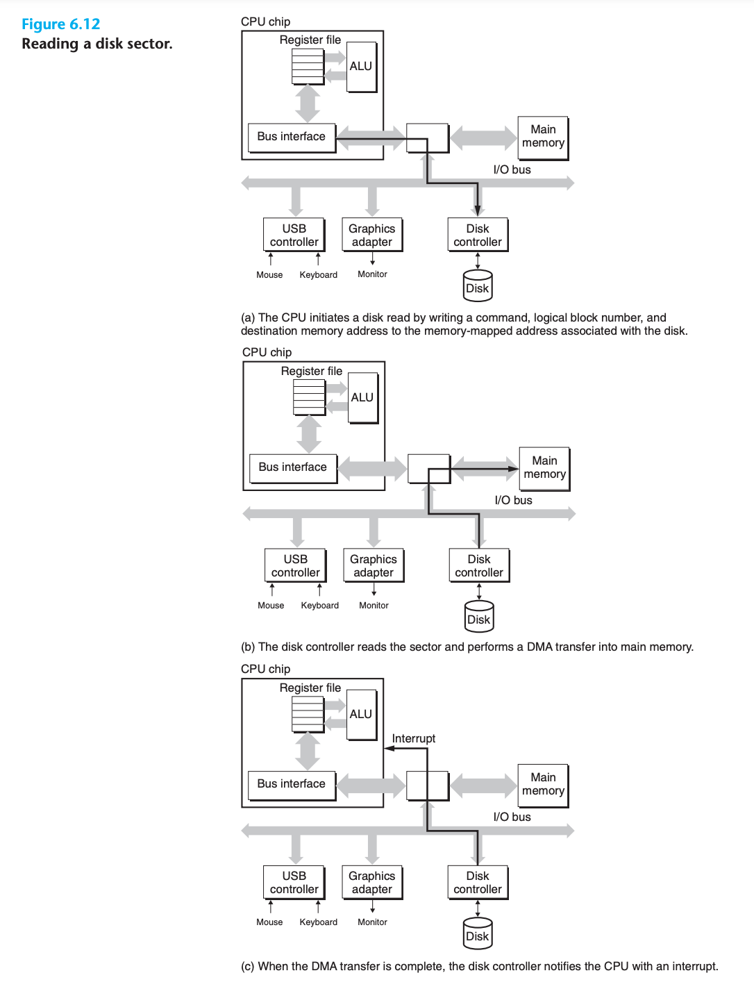
The CPU issues commands to I/O devices using a technique called memory mapped I/O
- In a system with memory-mapped I/O, a block of addresses in the address space is reserved for communicating with I/O devices.
- Each of these addresses is known as an I/O port.
- Each device is associated with (or mapped to) one or more ports when it is attached to the bus
As a simple example, suppose that the disk controller is mapped to port 0xa0.
- The CPU initiates a disk read by executing three store instructions to address
0xa0- The first of instruction sends a command word that tells the disk to initiate a read, along with other parameters such as whether to interrupt the CPU when the read is finished
- The second instruction indicates the logical block number that should be read.
- The third instruction indicates the main memory address where the contents of the disk sector should be stored
- After it issues the request, the CPU will typically do other work while the disk is performing the read
- CPU is much faster than disk, waiting is wasteful
- Disk can do its job without intervention of CPU
- Disk controller transfer logical memory address to physical memory address
- Reads the contents of the sector, and transfers the contents directly to main memory
- This process, whereby a device performs a read or write bus transaction on its own, without any involvement of the CPU, is known as direct memory access (DMA). The transfer of data is known as a DMA transfer.
- When the data transmission is completed, the disk controller notices the CPU with an interruption
- The basic idea is that an interrupt signals an external pin on the CPU chip.
- This causes the CPU to stop what it is currently working on and jump to an operating system routine.
- The routine records the fact that the I/O has finished and then returns control to the point where the CPU was interrupted.
6.1.3 Solid State Disks
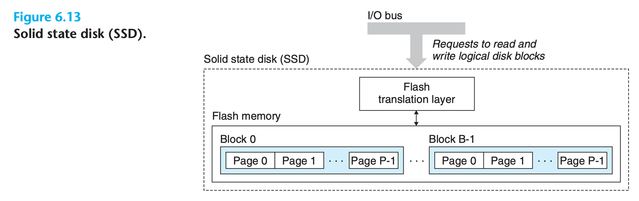
A solid state disk is a storage technology, based on flash memory
- An SSD package consists of one or more flash memory chips
- A flash translation layer, which is a hardware/firmware device that plays the same role as a disk controller, translating requests for logical blocks into accesses of the underlying physical device
- Notice that reading from SSDs is faster than writing. The difference between random reading and writing performance is caused by a fundamental property of the underlying flash memory
- a flash memory consists of a sequence of B blocks, where each block consists of P pages. Data are read and written in units of pages.
- A page can be written only after the entire block to which it belongs has been erased.
- However, once a block is erased, each page in the block can be written once with no further erasing. A block wears out after roughly 100,000 repeated writes. Once a block wears out, it can no longer be used.
- Manufacturers have developed sophisticated logic in the flash translation layer that attempts to amortize the high cost of erasing blocks and to minimize the number of internal copies on writes
Disadvantages of SSD
First, because flash blocks wear out after repeated writes, SSDs have the potential to wear out as well
(Wear-leveling logic in the flash translation layer attempts to maximize the lifetime of each block by spreading erasures evenly across all blocks. In practice, the wear-leveling logic is so good that it takes many years for SSDs to wear out )
HDD can be rewritten much more times
Practice Problem 6.5
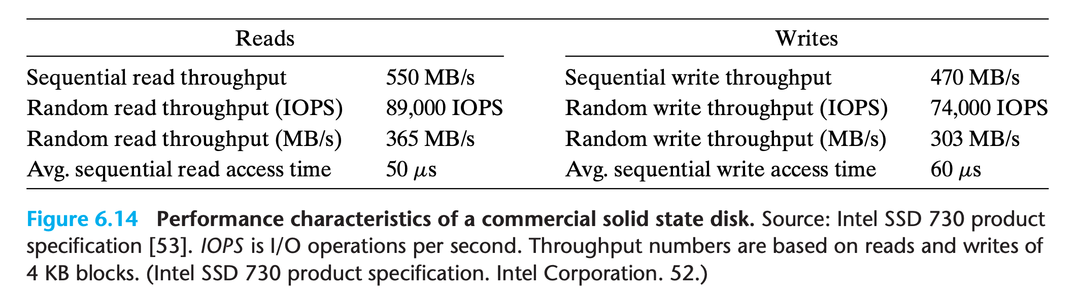
As we have seen, a potential drawback of SSDs is that the underlying flash memory can wear out. For example, for the SSD in Figure 6.14, Intel guarantees about 128 petabytes ($128 × 10^{15}$ bytes) of writes before the drive wears out. Given this assumption, estimate the lifetime (in years) of this SSD for the following workloads:
A. Worst case for sequential writes: The SSD is written to continuously at a rate of 470 MB/s (the average sequential write throughput of the device).
B. Worst case for random writes: The SSD is written to continuously at a rate of 303 MB/s (the average random write throughput of the device).
C. Average case: The SSD is written to at a rate of 20 GB/day (the average daily write rate assumed by some computer manufacturers in their mobile computer workload simulations).
My solution : :white_check_mark:
1 | wear_out_limit = 128 * 10 ** 15 |
So even if the SSD operates continuously, it should last for at least 8 years, which is longer than the expected lifetime of most computers.
6.2 Locality
Well written programs tend to reference data items that are near other recently referenced data items or that were recently referenced themselves
Locality is typically described as having two distinct forms: temporal locality and spatial locality.
- In a program with good temporal locality, a memory location that is referenced once is likely to be referenced again multiple times in the near future.
- In a program with good spatial locality, if a memory location is referenced once, then the program is likely to reference a nearby memory location in the near future.
6.2.1 Locality of References to Program Data
6.2.2 Locality of Instruction Fetches
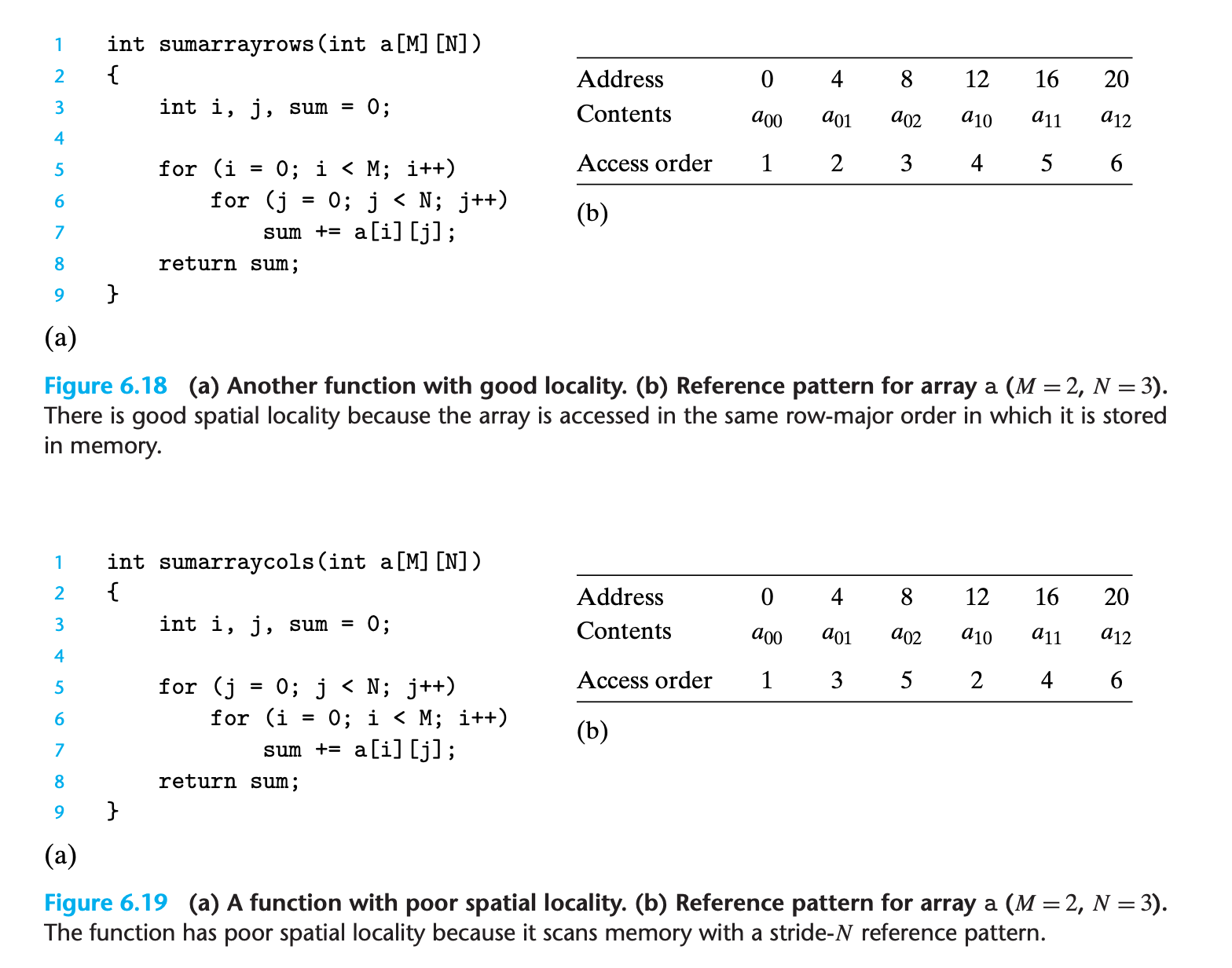
For example, in Figure 6.18 the instructions in the body of the for loop are executed in sequential memory order, and thus the loop enjoys good spatial locality. Since the loop body is executed multiple times, it also enjoys good temporal locality.
An important property of code that distinguishes it from program data is that it is rarely modified at run time.
6.2.3 Summary of Locality
- Programs that repeatedly reference the same variables enjoy good temporal locality.
- . For programs with stride-k reference patterns, the smaller the stride, the better the spatial locality. Programs with stride-1 reference patterns have good spatial locality. Programs that hop around memory with large strides have poor spatial locality
- Loops have good temporal and spatial locality with respect to instruction fetches. The smaller the loop body and the greater the number of loop iterations, the better the locality
Practice Problem 6.7
Permute the loops in the following function so that it scans the three-dimensional array a with a stride-1 reference pattern.
2
3
4
5
6
7
8
9
10
11
12
13
{
int i, j, k, product = 1;
for (i = N-1; i >= 0; i--) {
for (j = N-1; j >= 0; j--) {
for (k = N-1; k >= 0; k--) {
product *= a[j][k][i];
}
}
}
return product;
}
My solution : :white_check_mark:
1 | int productarray3d(int a[N][N][N]) |
Practice Problem 6.8
The three functions in Figure 6.20 perform the same operation with varying degrees of spatial locality. Rank-order the functions with respect to the spatial locality enjoyed by each. Explain how you arrived at your ranking.
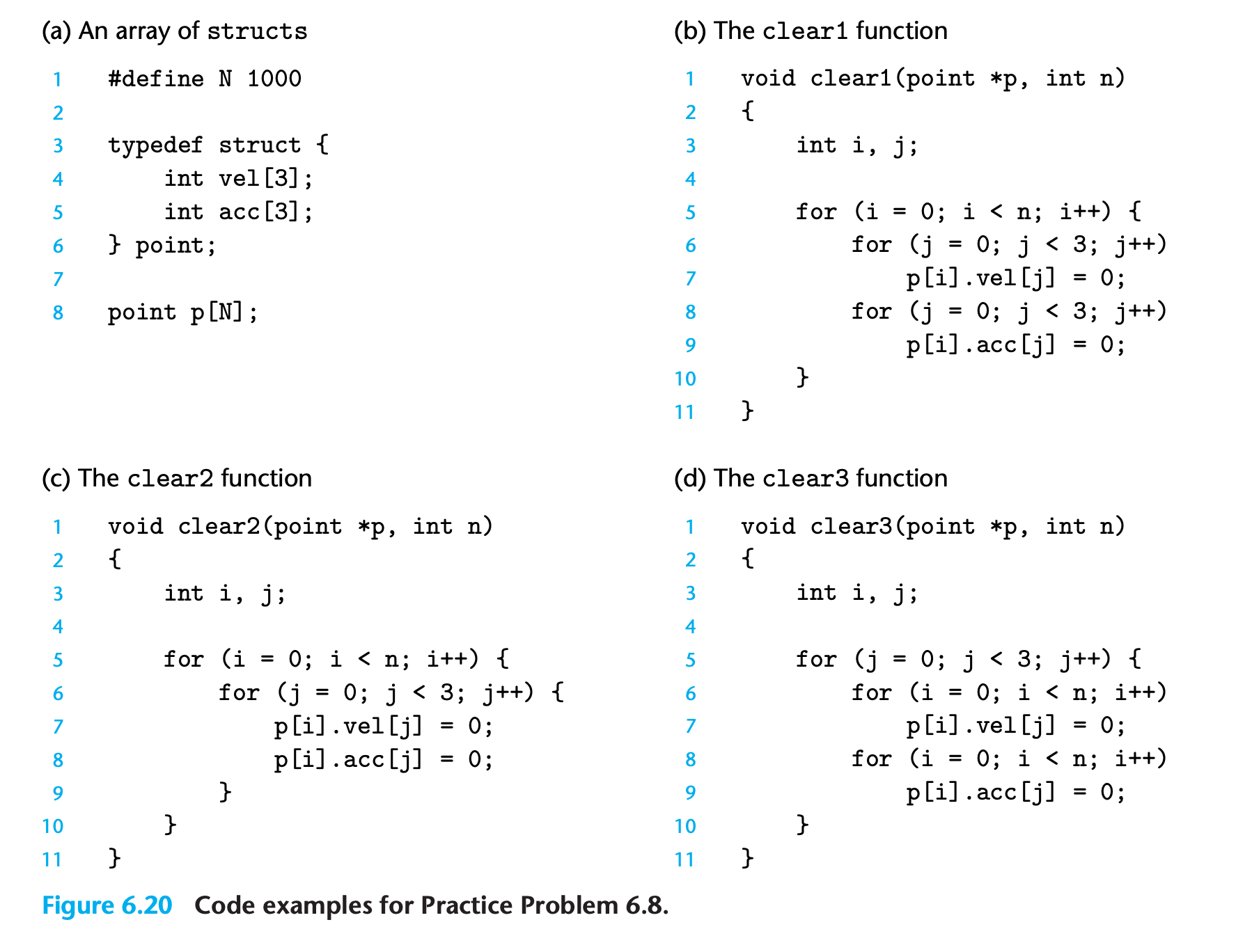
My solution : :white_check_mark:
1 | clear1 > clear2 > clear3 |
6.3 The Memory Hierarchy
6.3.1 Caching in the Memory Hierarchy
In general, a cache is a small, fast storage device that acts as a staging area for the data objects stored in a larger, slower device.
Each level in the hierarchy caches data objects from the next lower level.
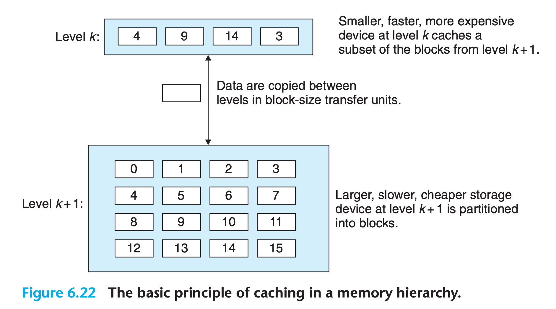
Data exchange in unit of block
- the size of a block can be both fixed and variable
- all data blocks in level k can be found in level k+1
- In general, devices lower in the hierarchy have longer access times, and thus tend to use larger block sizes in order to amortize these longer access times.
Cache Hits
When a program needs a particular data object d from level k + 1, it first looks for d in one of the blocks currently stored at level k.
If d happens to be cached at level k, then we have what is called a cache hit.
Cache Misses
If, on the other hand, the data object d is not cached at level k, then we have what is called a cache miss.
When there is a miss, the cache at level k fetches the block containing d from the cache at level k + 1, possibly overwriting an existing block if the level k cache is already full(known as replacing or evicting the block.The block that is evicted is sometimes referred to as a victim block).
The decision about which block to replace is governed by the cache’s replacement policy
- For example, a cache with a random replacement policy would choose a random victim block.
- A cache with a least recently used (LRU)replacement policy would choose the block that was last accessed the furthest in the past
Notice that the program/CPU will never access the k+1 level directly, it is the job of cache to fetch the missing data!
Cache Management
Something has to partition the cache storage into blocks, transfer blocks between different levels, decide when there are hits and misses, and then deal with them.
The logic that manages the cache can be hardware, software, or a combination of the two
For example, the compiler manages the register file, the highest level of the cache hierarchy. It decides when to issue loads when there are misses, and determines which register to store the data in. The caches at levels L1, L2, and L3 are managed entirely by hardware logic built into the caches.
In a system with virtual memory, the DRAM main memory serves as a cache for data blocks stored on disk, and is managed by a combination of operating system software and address translation hardware on the CPU
6.3.2 Summary of Memory Hierarchy Concepts
To summarize, memory hierarchies based on caching work because slower storage is cheaper than faster storage and because programs tend to exhibit locality
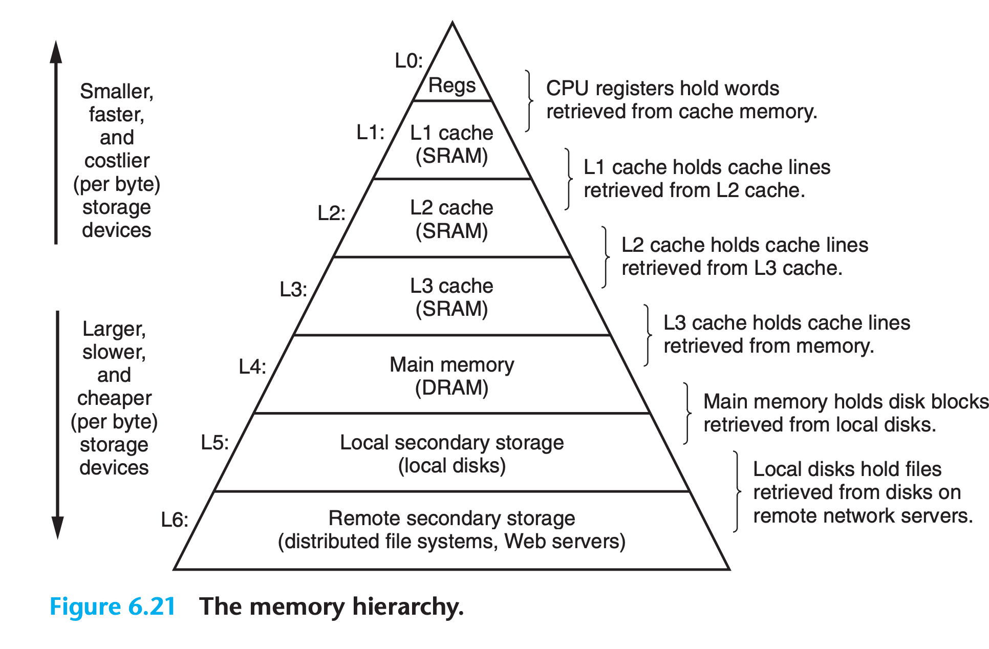
6.4 Cache Memories
The memory hierarchies of early computer systems consisted of only three levels: CPU registers, main memory, and disk storage
However, because the increasing gap between CPU and main memory, designers have to insert caches
- L1 cache, just below register files, can be accessed nearly as fast as the registers
- L2 cache, below L1 cache
- L3 cache, below L2 cache
- ….
While there is considerable variety in the arrangements, the general principles are the same.
For our discussion in the next section, we will assume a simple memory hierarchy with a single L1 cache between the CPU and main memory
6.4.1 Generic Cache Memory Organization
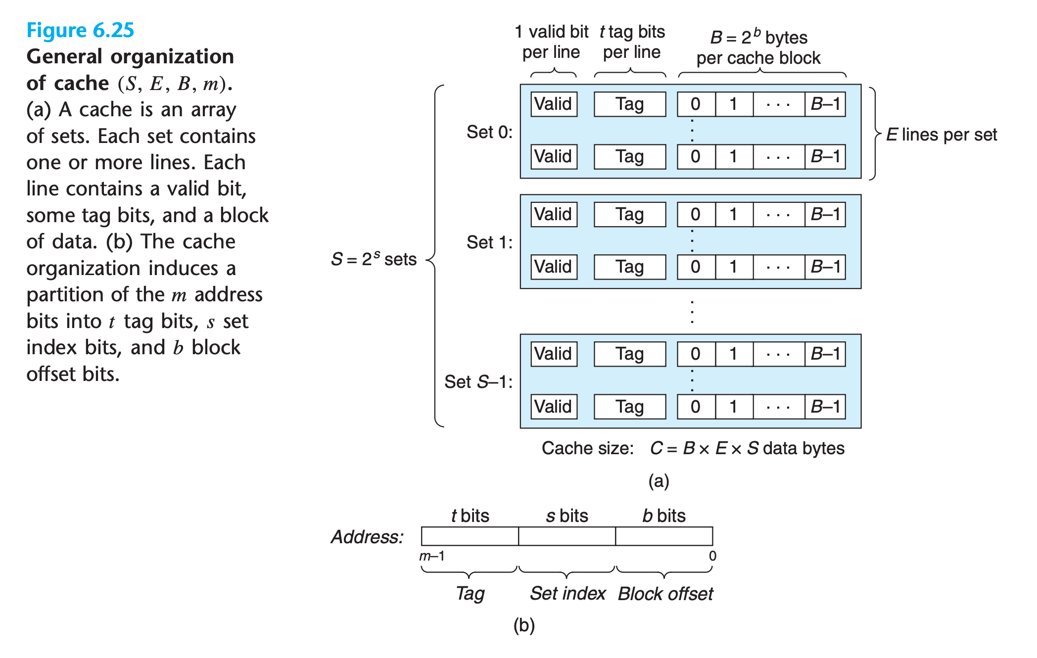
Consider a computer system where each memory address has $m$ bits
- a cache is organized as an array of $S = 2^s$ cache sets
- Each set consists of E cache lines.
- Each line consists of
- a data block of $B = 2^b$ bytes
- a valid bit that indicates whether or not the line contains meaningful information
- $t = m − (b + s)$ tag bits (a subset of the bits from the current block’s memory address) that uniquely identify the block stored in the cache line.
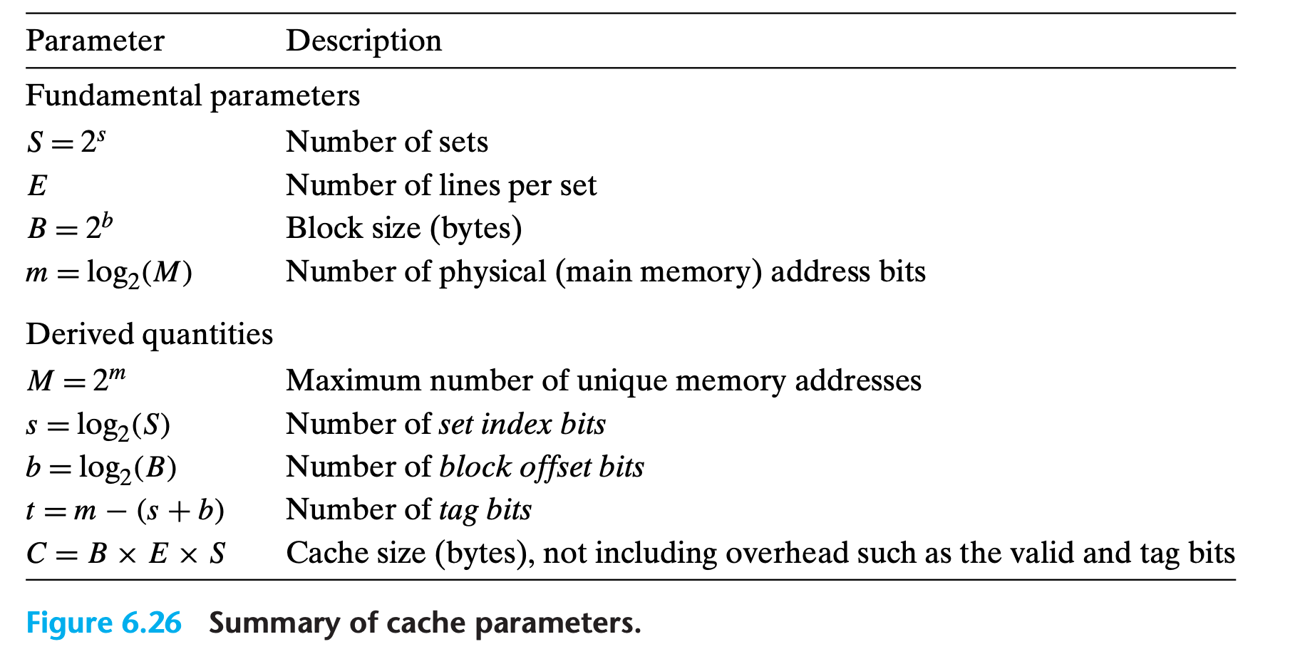
In general, a cache’s organization can be characterized by the tuple $(S, E, B, m)$
The size (or capacity) of a cache, C, is stated in terms of the aggregate size of all the blocks. The tag bits and valid bit are not included. Thus, $C = S × E × B$.
How does the cache know whether it contains a copy of the word at address A ?
The cache is organized so that it can find the requested word by simply inspecting the bits of the address, similar to a hash table with an extremely simple hash function
Given $s ,b$ and partition of memory address $m$ as $t$
1 | def cache_match(s,b,t): |
Practice Problem 6.9
The following table gives the parameters for a number of different caches. For each cache, determine the number of cache sets (S), tag bits (t), set index bits (s), and block offset bits (b).
Cache m C B E S t s b 1 32 1024 4 1 2 32 1024 8 4 3 32 1024 32 32
My solution : :white_check_mark:
1 | from math import log |
| Cache | m | C | B | E | S | t | s | b |
|---|---|---|---|---|---|---|---|---|
| 1 | 32 | 1024 | 4 | 1 | 256 | 22 | 8 | 2 |
| 2 | 32 | 1024 | 8 | 4 | 32 | 24 | 5 | 3 |
| 3 | 32 | 1024 | 32 | 32 | 1 | 27 | 0 | 5 |
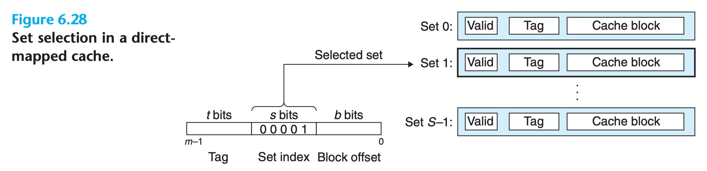
6.4.2 Direct-Mapped Caches
A cache with exactly one line per set (E = 1) is known as a direct-mapped cache
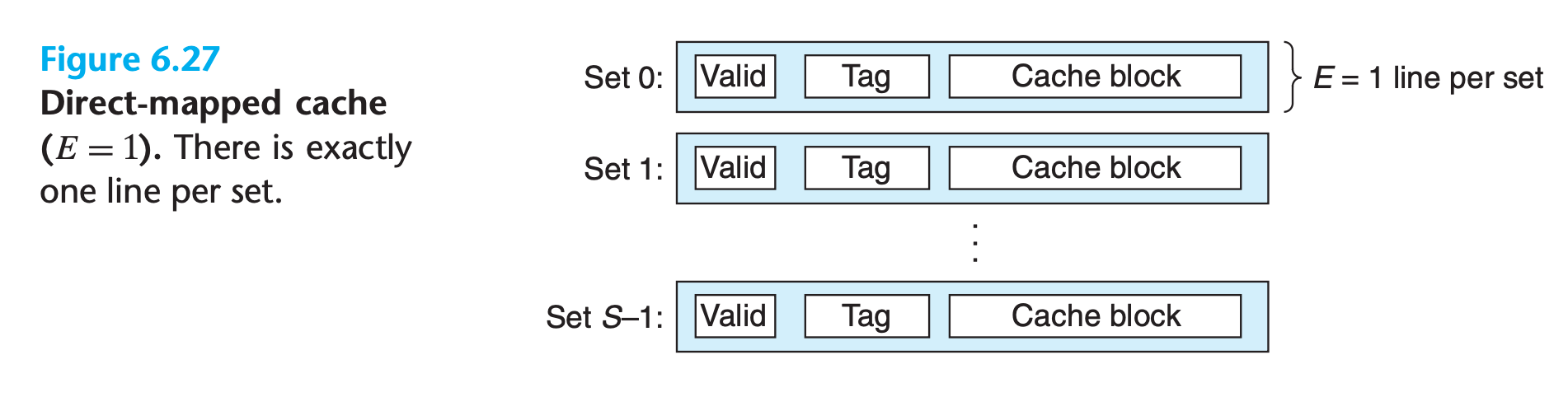
The process that a cache goes through of determining whether a request is a hit or a miss and then extracting the requested word consists of three steps: (1) set selection, (2) line matching, and (3) word extraction.
Set Selection in Direct-Mapped Caches
In this step, the cache extracts the s set index bits from the middle of the address for w. These bits are interpreted as an unsigned integer that corresponds to a set number
Line Matching in Direct-Mapped Caches
The next step is to determine if a copy of the word w is stored in one of the cache lines contained in set i.
In a direct-mapped cache, this is easy and fast because there is exactly one line per set.
1 | def cache_hit(selected_set , t): |
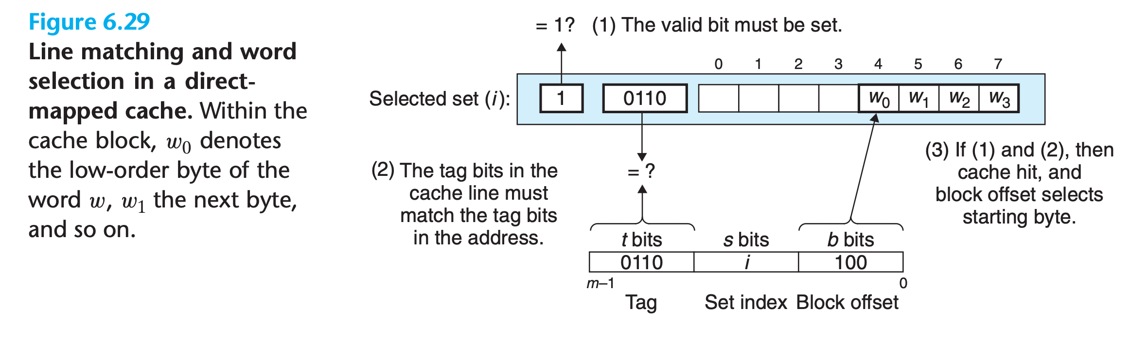
Word Selection in Direct-Mapped Caches
Once we have a hit, we know that w is somewhere in the block.
As shown in Figure 6.29, the block offset bits provide us with the offset of the first byte in the desired word
Line Replacement on Misses in Direct-Mapped Caches
If the cache misses, then it needs to retrieve the requested block from the next level in the memory hierarchy and store the new block in one of the cache lines of the set indicated by the set index bits
In general, if the set is full of valid cache lines, then one of the existing lines must be evicted.
For a direct-mapped cache, the current line is replaced by the newly fetched line.
Putting It Together: A Direct-Mapped Cache in Action
it can be very instructive to enumerate the entire address space and partition the bits
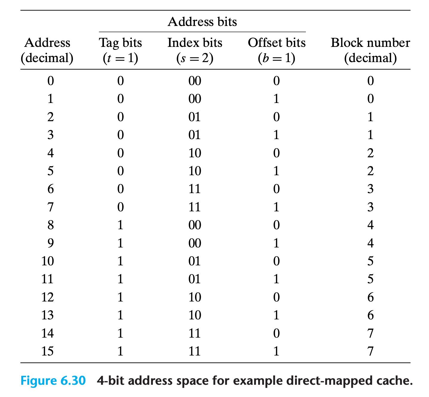
Notice that the concatenation of the tag and index bits uniquely identifies each block in memory.
Also
bin(address) == str(t)+str(s)+str(b)
Conflict Misses in Direct-Mapped Caches
Conflict misses are common in real programs and can cause baffling performance problems
Conflict miss is where we have plenty of room in the cache but keep alternating references to blocks that map to the same cache set
For example, if we only have a 2 set direct mapped cache and x is contiguous with y
1 | float dotprod(float x[8], float y[8]) |
We will have the following memory address map (suppose x begins at address 0)
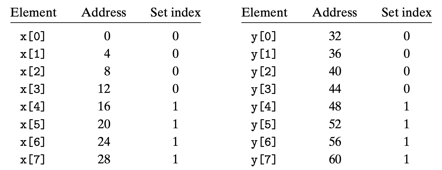
We first refers x[0], load it into cache, and then refers to y[0], throw x[0] out
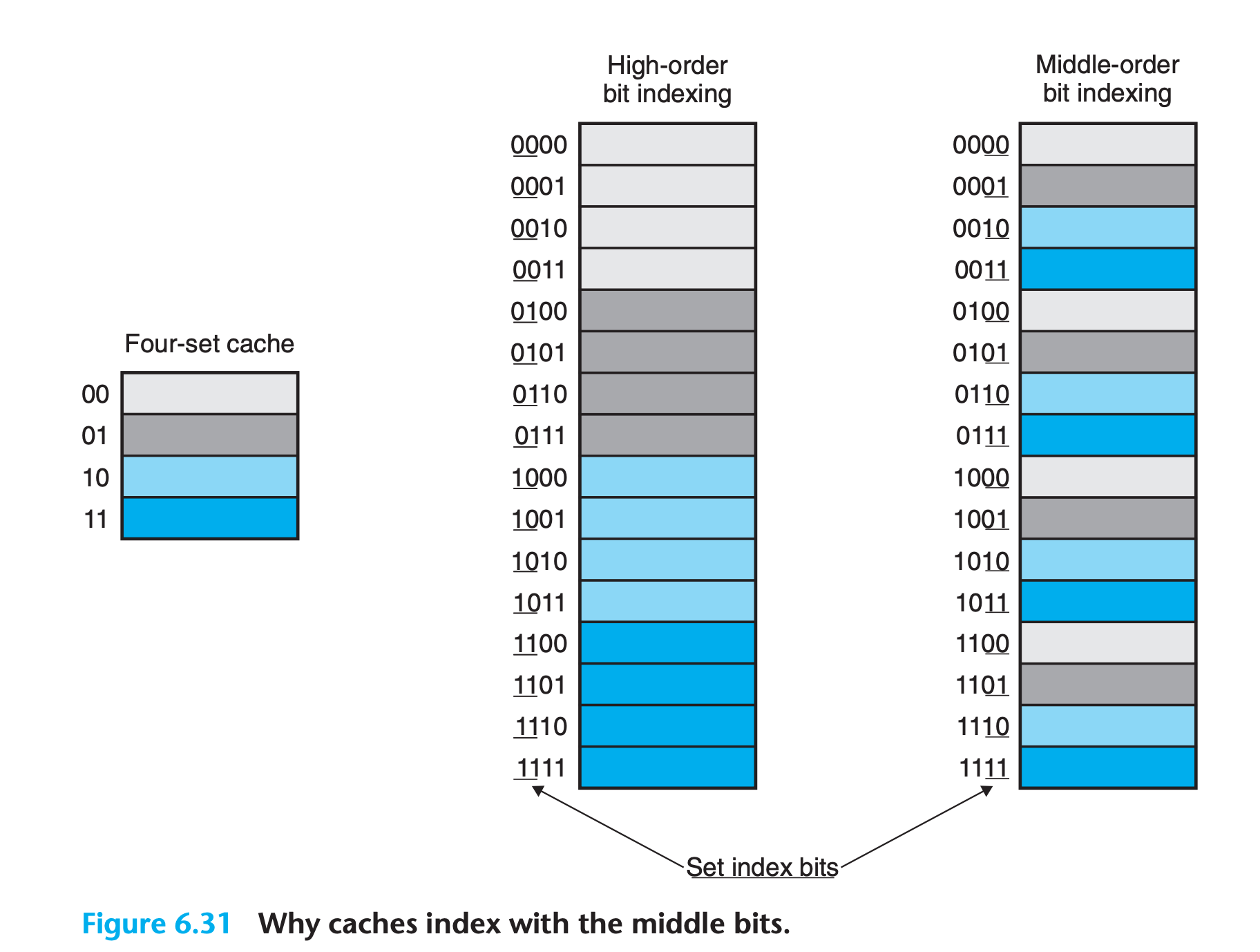
You may be wondering why caches use the middle bits for the set index instead of the high-order bits. There is a good reason why the middle bits are better. Figure 6.31 shows why. If the high-order bits are used as an index, then some contiguous memory blocks will map to the same cache set
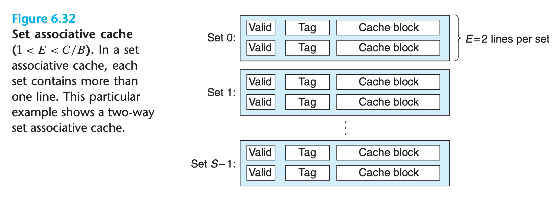
6.4.3 Set Associative Caches
The problem with conflict misses in direct-mapped caches stems from the constraint that each set has exactly one line
A set associative cache relaxes this constraint so that each set holds more than one cache line. A cache with $1 < E < C/B$ is often called an E-way set associative cache.
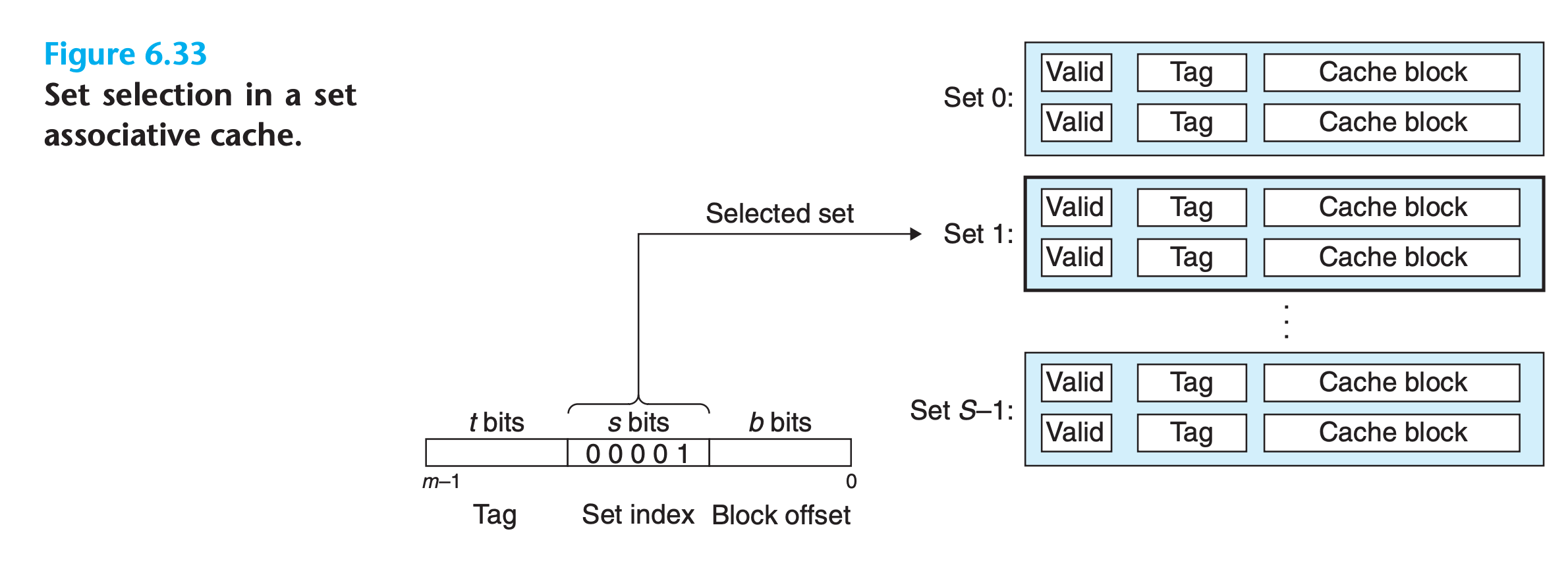
Set Selection in Set Associative Caches
Set selection is identical to a direct-mapped cache
Line Matching and Word Selection in Set Associative Caches
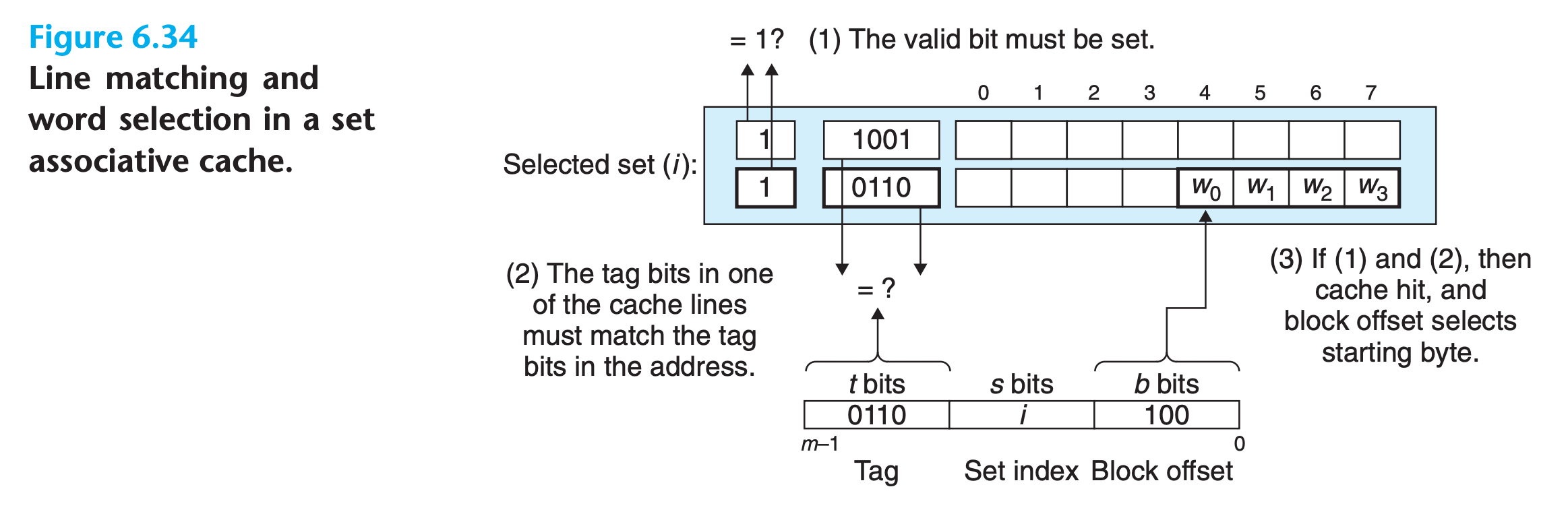
- It must check the tags and valid bits of multiple lines in order to determine if the requested word is in the set
- It uses a technique called associative memory which functions like a Python dictionary(It can compare all lines in the set at the same time rather than ask them one by one!)
1 | # assume all valid bits are 1 |
Line Replacement on Misses in Set Associative Caches
When there is a cache miss which line should it replace ?
It is very difficult for programmers to exploit knowledge of the cache replacement policy in their codes, so we will not go into much detail about it here
- The simplest replacement policy is to choose the line to replace at random
- Other more sophisticated policies can be applied are least frequently used (LFU), least recently used (LRU) and so on
6.4.4 Fully Associative Caches
A fully associative cache consists of a single set (i.e., $E = C/B$) that contains all of the cache lines
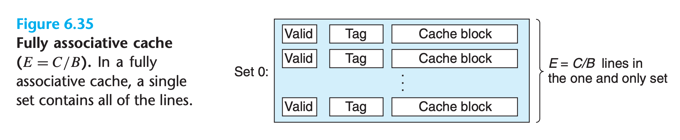
Set Selection in Fully Associative Caches
Set selection in a fully associative cache is trivial because there is only one set, no need to select
Line Matching and Word Selection in Fully Associative Caches
Line matching and word selection in a fully associative cache work the same as with a set associative cache
Because the cache circuitry must search for many matching tags in parallel, it is difficult and expensive to build an associative cache that is both large and fast
As a result, fully associative caches are only appropriate for small caches, such as the translation lookaside buffers (TLBs) in virtual memory systems that cache page table entries
6.4.5 Issues with Writes
After the cache updates its copy of w, what does it do about updating the copy of w in the next lower level of the hierarchy?
- Write-through
- immediately write w’s cache block to the next lower level.
- has the disadvantage of causing bus traffic with every write
- Write-back
- only when it is evicted from the cache by the replacement algorithm does it write back to memory
- Because of locality, write-back can significantly reduce the amount of bus traffic
- The cache must maintain an additional dirty bit for each cache line that indicates whether or not the cache block has been modified.
Another issue is how to deal with write misses
- Write-allocate
- loads the corresponding block from the next lower level into the cache and then updates the cache block
- has the disadvantage that every miss results in a block transfer from the next lower level to the cache
- No-write-allocate
- bypasses the cache and writes the word directly to the next lower level.
Write-through caches are typically no-write-allocate. Write-back caches are typically write-allocate
To the programmer trying to write reasonably cache-friendly programs, we suggest adopting a mental model that assumes write-back, write-allocate caches
- As a rule, caches at lower levels of the memory hierarchy are more likely to use writeback instead of write-through because of the larger transfer times
- It is symmetric to the way reads are handled, in that write-back write-allocate tries to exploit locality
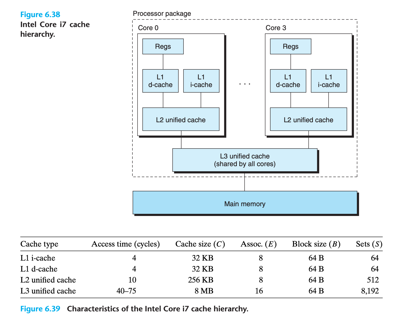
6.4.6 Anatomy of a Real Cache Hierarchy
A cache that holds instructions only is called an i-cache.
A cache that holds program data only is called a d-cache.
A cache that holds both instructions and data is known as a unified cache.
Modern processors include separate i-caches and d-caches.
6.4.7 Performance Impact of Cache Parameters
Cache performance is evaluated with a number of metrics:
Miss rate
The fraction of memory references during the execution of a program, or a part of a program, that miss
$$
miss\ rate = \frac{miss \ times}{total \ times}
$$Hit rate
The fraction of memory references that hit.
$$
hit \ rate = 1 - miss \ rate
$$Hit time.
The time to deliver a word in the cache to the CPU, including the time for set selection, line identification, and word selection.
Miss penalty.
Any additional time required because of a miss. The penalty for L1 misses served from L2 is on the order of 10 cycles; from L3, 50 cycles; and from main memory, 200 cycles.
6.5 Writing Cache-Friendly Code
Programs with better locality will tend to have lower miss rates, and programs with lower miss rates will tend to run faster than programs with higher miss rates.
- Repeated references to local variables are good because the compiler can cache them in the register file (temporal locality).
- Stride-1 reference patterns are good because caches at all levels of the memory hierarchy store data as contiguous blocks (spatial locality).
The famous example illustrate this :
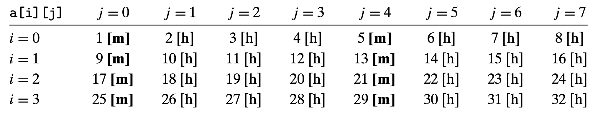
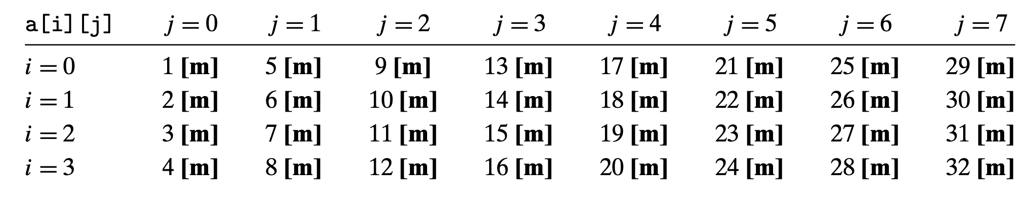
1 | int sumarrayrows(int a[M][N]) |
(C stores arrays in row-major order)
Row major miss rate
Column major miss rate
Practice Problem 6.17
Transposing the rows and columns of a matrix is an important problem in signal processing and scientific computing applications. It is also interesting from a locality point of view because its reference pattern is both row-wise and column-wise. For example, consider the following transpose routine:
2
3
4
5
6
7
8
9
10
11
12
void transpose1(array dst, array src)
{
int i, j;
for (i = 0; i < 2; i++) {
for (j = 0; j < 2; j++) {
dst[j][i] = src[i][j];
}
}
}Assume this code runs on a machine with the following properties:
sizeof(int) == 4- The src array starts at address 0 and the dst array starts at address 16 (decimal).
- There is a single L1 data cache that is direct-mapped, write-through, and write-allocate, with a block size of 8 bytes.
- The cache has a total size of 16 data bytes and the cache is initially empty.
- Accesses to the src and dst arrays are the only sources of read and write misses, respectively.
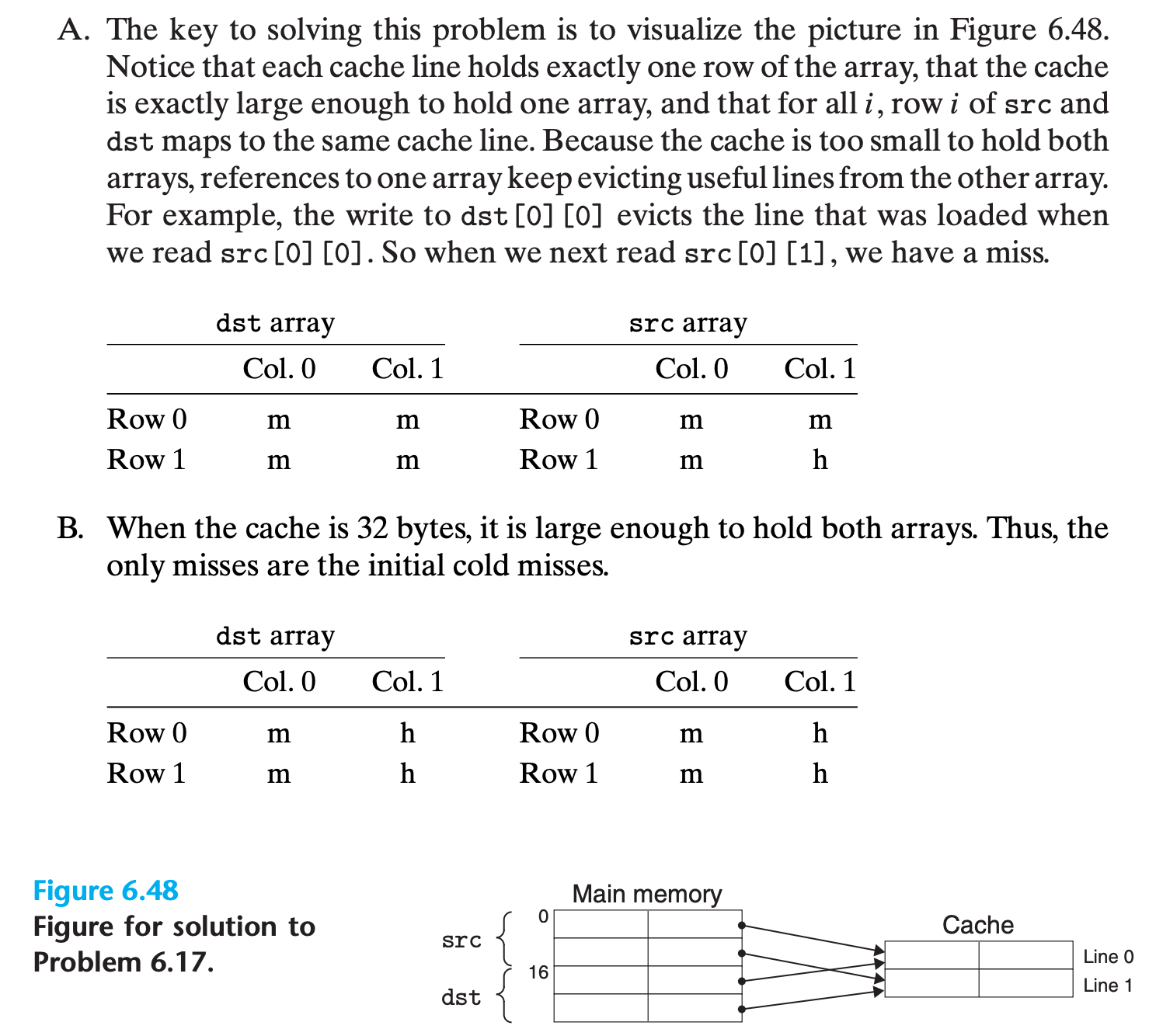
A. For each
rowandcol, indicate whether the access tosrc[row][col]anddst[row][col]is a hit (h) or a miss (m). For example, readingsrc[0][0]is a miss and writingdst[0][0]is also a miss.
2
3
4
5
6
7
8
9
| src | dest |
+----+-------+----------+----+----------+-------+
| |col0 | col1 | | col0 | col1 |
+----+-------+----------+----+----------+-------+
|row0| m | |row0| | |
+----+-------+----------+----+----------+-------+
|row1| | |row1| | |
+----+-------+----------+----+----------+-------+B. Repeat the problem for a cache with 32 data bytes.
My solution : :x:
A
1 | +-----------------------+-----------------------+ |
B
1 | +-----------------------+-----------------------+ |
Solution on the book:
6.6 Putting It Together: The Impact of Caches on Program Performance
This section wraps up our discussion of the memory hierarchy by studying the impact that caches have on the performance of programs running on real machines.
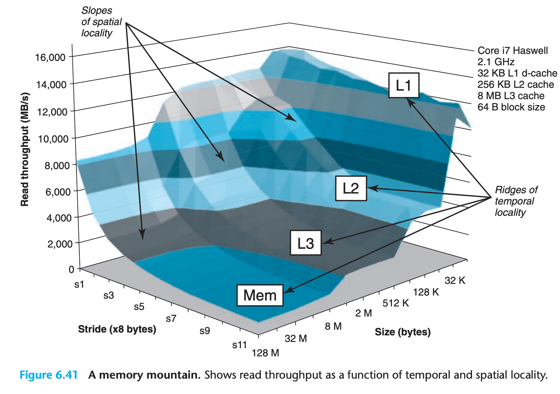
6.6.1 The Memory Mountain
6.6.2 Rearranging Loops to Increase Spatial Locality
6.6.3 Exploiting Locality in Your Programs
- . Focus your attention on the inner loops, where the bulk of the computations and memory accesses occur.
- Try to maximize the spatial locality in your programs by reading data objects sequentially, with stride 1, in the order they are stored in memory
- Try to maximize the temporal locality in your programs by using a data object as often as possible once it has been read from memory.
6.7 Summary
Being able to look at code and get a qualitative sense of its locality is a key skill for a professional programmer
cache memory is completely managed by hardware
When working with arrays it is helpful to draw an access graph
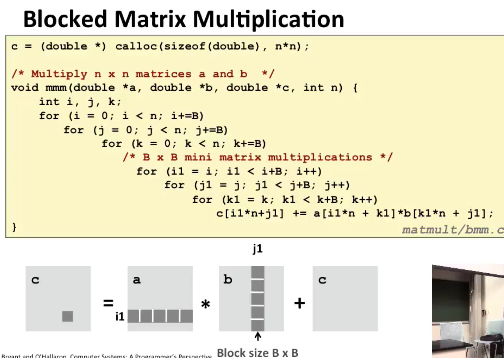
Using blocking to increase temporal locality
There is an interesting technique called blocking that can improve the temporal locality of inner loops. The general idea of blocking is to organize the data structures in a program into large chunks called blocks. (In this context, “block” refers to an application-level chunk of data, not to a cache block.) The program is structured so that it loads a chunk into the L1 cache, does all the reads and writes that it needs to on that chunk, then discards the chunk, loads in the next chunk, and so on. Unlike the simple loop transformations for improving spatial locality, blocking makes the code harder to read and understand. For this reason, it is best suited for optimizing compilers or frequently executed library routines. Blocking does not improve the performance of matrix multiply on the Core i7, because of its sophisticated prefetching hardware. Still, the technique is interesting to study and understand because it is a general concept that can produce big performance gains on systems that don’t prefetch.